
Utilizing our 35 years of experience in optoelectronics, Marktech’s customization process focuses on customer needs and applications. Instead of using standardized–but perhaps non-optimized–parts, Marktech allows advantageous custom product variations to enhance your product design. Marktech provides the designer with insights concerning custom variations–variations that optimize mechanical, electrical, optical, and thermal characteristics without the need for large volume commitments. With manufacturing facilities in California and Japan, Marktech is a vertically-integrated company, allowing us to produce emitter and detector components quickly, thus decreasing your time to market. We can even produce your entire package in the United States.
To solve your needs, Marktech engineers will discuss with you:
- Application needs specific to your project
- Optimization of component and assembly packaging, technology,thermal, and electrical parameters
- Manufacturing of dedicated end-products in support of your specifications and needs
Overview
Once the emitter and/or detector electrical characteristics and chip sizes are determined (as discussed in earlier parts of this series), packaging design for these devices is needed in order to meet the goals of optical efficiency (along with viewing/radiation angle), space constraints, heat dissipation (and resultant reliability), electromagnetic interference, and product cost. The finished design is then prototyped and then electrically and environmentally screened as required.
Packaging provides the necessary interface between the semiconductors and the physical world to provide optimal electro-optical performance as well as the physical strength and reliability of the device. Optical designs maximize light output and power transfer for the desired viewing angle. Packaging can contribute 50 to 80% of the manufacturing expense of the optoelectronic assemblies.
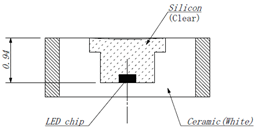
Optically clear silicones and epoxies are typically used for potting, molding, or encapsulation.
- Silicones are often used for high powered devices due to stable thermo-optical properties. Silicones are very stable in upper UV and blue light, even under high intensity, humidity, and temperature. They are also useful when incorporated into surface mount technology (SMT), where optical and mechanical stability are needed after exposure to solder reflow temperatures. Silicone attributes are: high transparency in the UV-visible region, controlled refractive index (RI), stable thermo</
- mechanical properties, and tunable hardness from soft gels to hard resins. A silicone can have a glass transition Tg below 0°C, but due to its flexibility and elasticity, it can be used at high and low temperature extremes.
- Epoxies are typically used for general purpose, low to medium power devices, and have a long history of use dating to the 1960-1970’s, with improvements in formulations along the way that have provided low cost and high reliability. The glass transition temperatures of epoxies are lower than for non-optical devices (65C is typical). High temperatures can cause mechanical stresses, as well as degrade light transmission over time.
Die attachment is typically provided by silver filled epoxy or, for more heat transfer by Direct Attachment (DA), Flip Chip attachment, or solder eutectic.
- Epoxy die attach material is silver filled to provide thermal and electrical conductivity. Additional desirable attributes are: low outgassing, low bleed, good adhesion characteristics, and high glass transition point (typical value: 140C).
- Direct Attachment (DA) employs an efficient flux eutectic bonding process for attaching chips without the use of epoxy. The technique uses a process which eliminates the need for solder paste, preforms or conductive adhesives (see below for more detail).
- Flip Chip die attach uses a solder bump bonding method (see below for more detail).
- Solder is used for some high power devices, but also as mentioned for Flip Chip chip on board (COB) use, where the controlled –collapse chip connection soldering allow self-alignment of devices as well other electro-mechanical advantages.
Substrate materials can be metal lead frames, standard TO style metal headers, ceramic headers, and printed circuit boards of FR4, ceramic construction, or metal core. Ceramic packaging is preferred when higher thermal stability is required, with low-temperature co-fired ceramic substrates in common use. Selection of materials to provide needed CTE (coefficient of thermal expansion) enhances the thermal path from the chip to the heat sink, thereby lowering the junction temperature of the chip and improving quality/ reliability.
Chemical compatibility with packaging materials should be reviewed with Marktech, as acids and solvents may not be compatible with reliable product use.
Temperature concerns
The development of high-power GaN visible chips for commercial use since the 1990’s (with >150 lumens per watt for LED’s replacing tungsten’s characteristics of 12 lumens/watt) have required an evolution from standard lead-frame/molded epoxy 5mm and similar lamps to allow for the heat generation and general power requirements of the newer high lumen output chips produced by Cree (and sold through Marktech for custom use). Evaluation Star and Linear boards from Marktech help in characterization of these products. Care is needed to not exceed maximum junction temperature specifications, and it is beneficial to derate the temperature of the parts for reliability. Thermal management is a key aspect of packaging for high-power LED’s. Overheating can decompose the silicone of the inner lens, which then can become corrosive. Overdriving can carbonize the inner lens above the LED. Thermal expansion can cause broken wire bonds or die attach separation.
LED manufacturing volumes are typically lower than for non-optoelectronic microelectronics, where shorter cure times are used for packaging, and where reflowing solder may extend temperatures to 200C. Many optoelectronic assemblies are damaged at temperatures between 100C to 125C. Solder temperature and duration must be in accordance with recommendations.
Thermal conductivities for varied assemblies (in Watts per meter x degree Kelvin):
- FR4 printed circuit board: 0.23 W/mK
- Alumina or LTCC (low temperature co-fired ceramic) board: 25 W/mK
- Metal-core copper heatsink board: 400 W/mK
- Flip chip LED’s with silicon backing: 150 W/mK
Alternatively, the following graph shows the progress in thermal efficiency for the newer packaging variations.
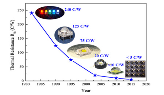
Thermal Resistance Comparison (Junction to Pad)
Customized assemblies
Customized assemblies can provide prototypes for what-if product builds, evaluation test products, and products incorporating specific emitter and detector chips needed for demanding customer applications. Note: Marktech works with the entire Cree dice line, and can provide customization of products incorporating any of this product. In addition, Marktech provides customization of Marktech’s own specialized visible, IR, and UV dice.
Customized assemblies use selected emitters, detectors, and packaging, as detailed below.
Examples of Customized Products
Customized emitters
These can consist of Cree and Marktech UV, visible, and NIR /SWIR (near infrared/ short wavelength infrared) chips.
These include:
- High-brightness and high-power LEDs
- Multichip emitters and chip-on-board packaging
- Infrared, ultraviolet, and visible LED emitters
- Single or multi-chip LED packages or modules for multiple wavelength applications
- Single or multiple LED die configurations
Available LED emitters have wavelengths varying from 280nm (UV) through visible (440 to 700nm) to short wavelength infrared (SWIR; up to 3000nm). Our online Product Selector Guide helps in the selection of emitter wavelengths, while also indicating compatible detectors. Tight binning by Marktech can provide uniform color characteristics to optimize the application and the mating detectors’ sensitivities, providing process-controlled, uniform product solutions.
Cree emitter dice custom assemblies
Cree dice can be custom packaged by Marktech for specific application needs. Marktech is one of only a small number of suppliers with this access to Cree dice. Marktech provides expertise in both Direct Attachment (DA) and (SA) type chips as well as Chip on Board assembly techniques. Cree is a major supplier of DA and SA chips.
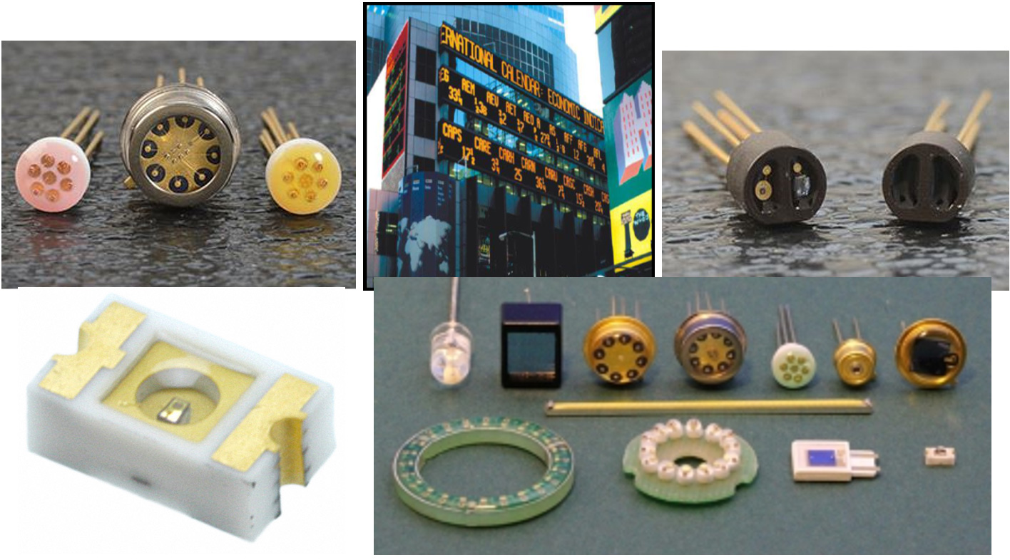
Customized detectors
Customized detectors are photo transistors and photodiodes with the ability to detect light in the UV, visible, and infrared spectrums.
These include:
- Standard photovoltaic silicon photodiodes
- Silicon photo transistor and Avalanche photodiodes
- Specialty photo detectors (including GaP Schottky)
- InGaAs and InP PIN photodiodes
- InGaAs/InP epitaxial wafers
- Silicon photodetectors (standard 400nm to 1100nm and new UV/Blue Enhanced 365nm – 1100nm): photovoltaic, photoconductive photodiodes, and phototransistors. Marktech’s silicon phototransistors can be utilized in applications requiring very high sensitivity, uniform response, and increased reliability such as card readers and optical sensors.
- Silicon avalanche photodiodes (400nm to 1100nm, with 800nm, 905nm optimization). Avalanche photodiodes (APDs) essentially provide an amplification gain stage through avalanche multiplication. They are similar to photomultipliers but are solid state semiconductor devices. Avalanche photodiodes are ideal for high-speed and low-light level detection in the near-infrared range. These detectors have become the semiconductor equivalent of photomultipliers in many applications including data communication, LIDAR, instrumentation, and photon counting. Marktech APDs have an internal gain mechanism, fast time response, low dark current, and high sensitivity in the near-infrared region. These APDs are recommended for applications that require high bandwidth or where internal gain is needed to overcome high pre-amp noise. In addition, these devices provide higher sensitivity than standard photodiodes and are ideal for extreme low-light level detection and short pulse detection.
- InGaAs PIN photodetectors (600nm to 2600nm). These are high-sensitivity and high-reliability products, ideally suited for optical communication devices. Chip active area sizes from 0.1mm to 3.0mm provide the optimum balance between low dark current, high speed, and light sensitivity, allowing for increased flexibility and options in a variety of applications ranging from fiber optics and high-speed optical communications to medical and chemical analysis. Marktech manufactures InP PIN photodiodes using InGaAs/InP technology, which have a spectral sensitivity in the 800nm to 2600nm range for applications requiring low dark current, high speed, and sensitivity such as fiber optics and optical communications. Marktech’s detector dice can be placed in a variety of packages from metal can TO-5, TO-18, and TO-46 to surface mount and standard 3mm and 5mm plastic packages. We can also incorporate the detector dice in custom-designed assemblies.
- SWIR (Short Wavelength IR) Emitters (1050nm to 1720nm): Marktech Optoelectronics is one of only a handful of manufacturers that supply emitters in the extended wavelength or SWIR range. Marktech’s standard product offering includes both through-hole and surface mount packages with wavelengths from 1050nm to 1720nm and operating currents ranging from 20mA to 350mA for high-power applications. Higher wavelength ranges up to 3000nm are available in specific package types. These detectors can be combined with a silicon sensor to cover the complete spectrum of light from the visible to the SWIR range.
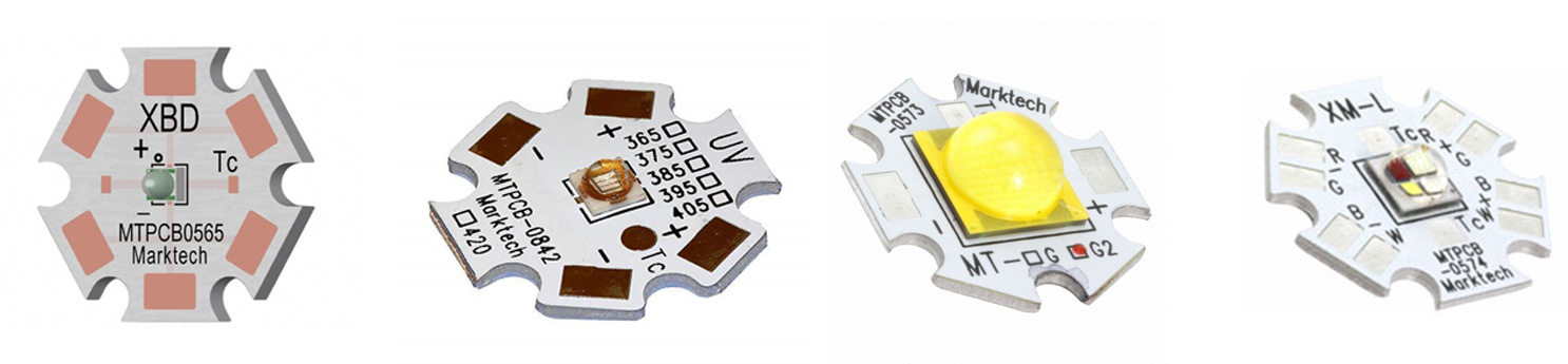
Marktech Custom Package Variations
Choose from any of the following package options when designing your custom emitter or detector component. These packages are designed for accommodating 1 – 7 chips in any configuration. If you don’t see a package that would work for your application, we can design a complete custom solution to meet your needs.
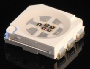
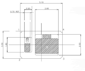
Ceramic Surface Mount Package with no added lens
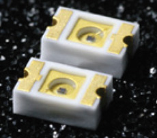
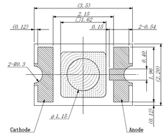
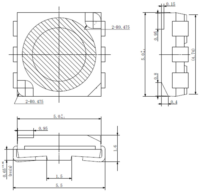
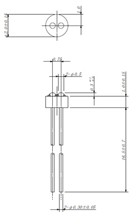
Plastic 6-leaded Surface Mount Package with no added lens
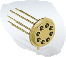
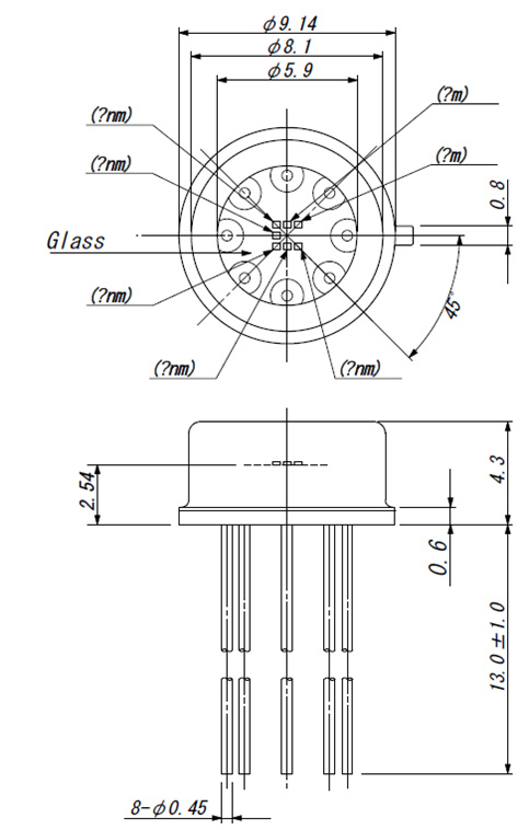
8 Pin, TO-39 Metal Can Package with multiple lens options
5mm ceramic stem with drip lens encapsulation
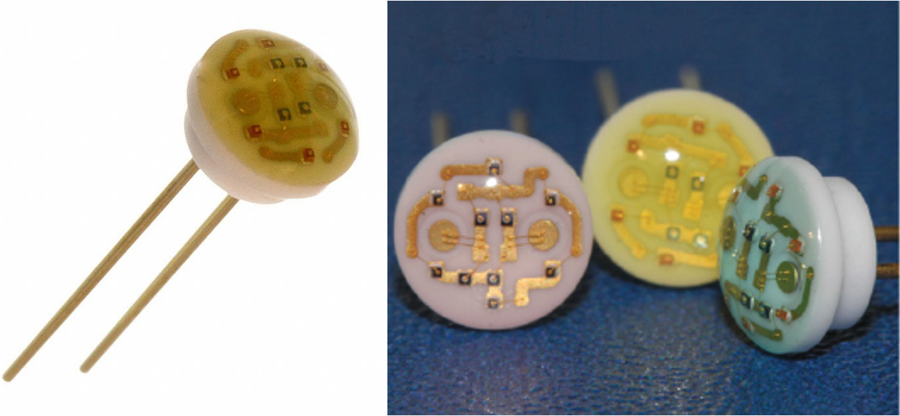
These versatile parts allow mix and matching of multiple emitters and multiple detectors.
Reflective Sensor Package for both emitter and detector
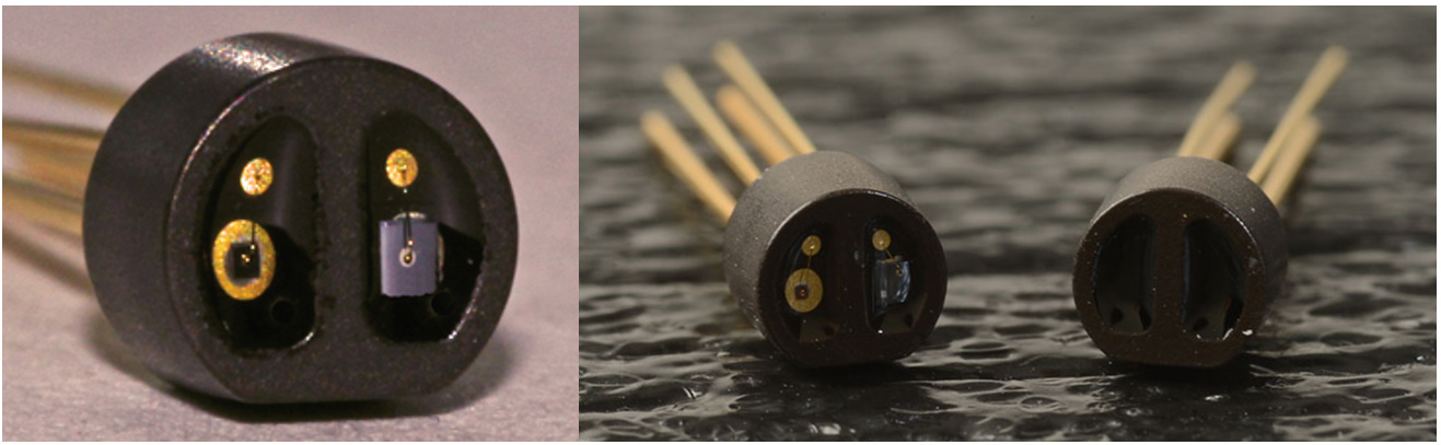
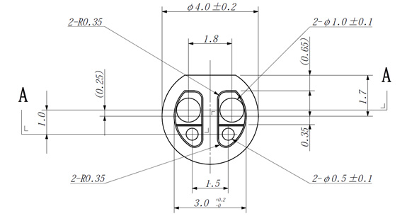
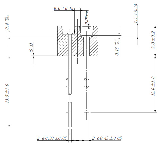
Custom designs are available for variations off of Marktech standard Photo Reflectors. Typically standard parts are offered in a compact high reliability 4mm plastic package with a wavelength range from 468nm to 950nm and optimal operational distance is 0.5mm-1.5mm. These devices offer superior alignment and sensitivity making them ideal for position sensing applications. Emitter/detector combinations are available from UV to SWIR.
Custom- COB (Chip-On-Board) mounting to FR-4 boards, metal core PCBs, and ceramic and flex Polyimide – up to 144 die on a single substrate.
In the late 2000’s, a push for even greater efficiency and increased density for LEDs was occurring, once again, primarily driven by the lighting and general illumination market. This resulted in the widespread introduction and usage of COB (Chip-On-Board) technology. COB is a semiconductor technology where the “chip” also referred to as the “die” is mounted directly on the printed circuit board using a procedure called die attach or die bonding. The individual die are placed on the PCB by either using a conductive paste or soldering (Eutectic) method and then wire bonded. This technology virtually eliminates the need for additional packaging such as lead frames and housings which allows for greater thermal dissipative qualities, reduced size and increased LED density (if required).
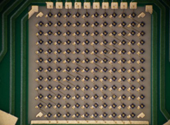
140pcs of a LED chip packaged into an area less than 1 square inch
There are still challenges with using COB technology especially from a manufacturing standpoint.
Some of these include:
(A) Capital expense – The equipment required is often very specialized and expensive
(B) Uniformity and consistency is critical in many COB applications, therefore, the bare Die / Chip must be carefully selected and tested prior to placement on the PCB. This process also requires very specialized equipment and in addition, the yields must be considered to maintain a cost effective device.
(C) Re-Work of COB assemblies can be difficult if already encapsulated. In some cases, the entire product must be discarded. If the product is able to be re-worked, typically, it can only be performed at the factory. Conversely, if the device is not encapsulated, re-work is relatively easy to perform compared to through-hole and SMT technology and less costly.
(D) The quality, uniformity and type of the PCB is critical to insure proper die attach and wire bond integrity. Pure, wire-bondable gold is often required if Direct Attach or Flip Chip techniques are not used.
COB technology is now being used by almost every major LED manufacturer, primarily in the general illumination and lighting marketplace. The increasing demand for energy efficient solutions to incandescent, halogen and similar antiquated technologies is allowing for rapid growth in the COB LED arena. As this technology continues to improve and costs decrease, the COB LED assembly market is expected to exceed the overall standard LED market in the next several years. Although most manufacturers are focused on energy efficient solutions to general illumination, there are a few select LED manufacturers (Marktech amongst them) who are using the many advantages of COB technology in more niche, highly specialized applications such as military, medical, machine vision and security.
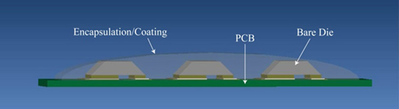
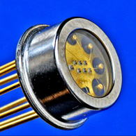
An offshoot of COB technology which further increases efficiency and provides an even greater opportunity for miniaturization are the Direct Attach and Flip Chip methods of assembly. Both methods do not require wire bonding thus allowing for a lower profile COB assembly while improving performance. Currently, a limited number of LED manufacturers (including Marktech) are taking advantage of this type of die structure. In addition, there are even a smaller number of assemblers that are capable of properly mounting this type of die. A major supplier of Direct Attach (DA) dice and the more recent (SA) dice is Cree, Inc. An example of one of their DA type chips is shown here.
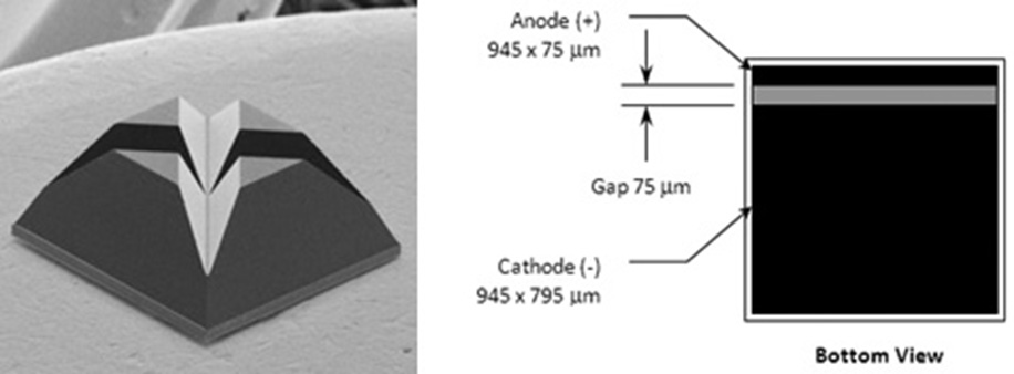
Direct Attach (DA) die top and bottom view
The Direct Attach technique uses a flux eutectic bonding process which eliminates the need for solder paste, preforms or conductive adhesives. An appropriate flux and PCB is all that is required to achieve a high quality bond during the re-flow process. An example of an assembly made with standard COB technology versus DA bonding is shown here.
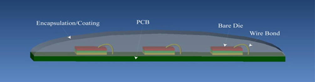
Standard COB assembly (Wire Bonding Required)
Direct Attach assembly (No Wire Bonding Required)
Flip chip technology flips over the LED in a face down orientation and places the electrodes in direct contact with the PCB. Like the Direct Attach process, this technology gives LED chips advantages that include a larger light-emitting area, better heat dissipation, along with eliminating the wire-bonding step and wire bond shadowing. The bonding method for flip chip die uses solder bumps. The attachment process consists of applying the appropriate type of flux (as in the DA method) to these solder bump areas and then performing a reflow process.
Due to the CTE (Coefficient of Thermal Expansion) mismatch between the flip chip and PCB, it is typically not recommended to use FR-4 material but a ceramic or optimized MC (Metal Core) substrate PCB.
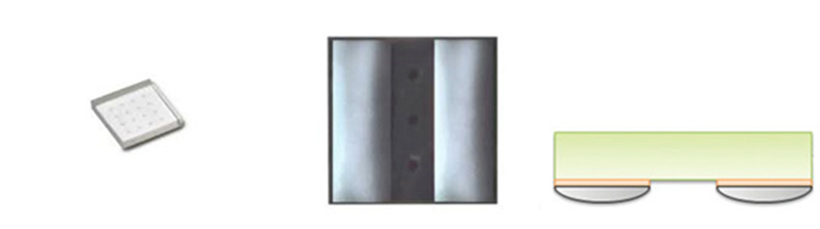
Flip Chip top view, bottom view and side view w/solder bumps
Both of these technologies are making large inroads into the general illumination and niche marketplaces mentioned previously. In addition to some of the advantages described earlier, the reduction in thermal resistance going from a through-hole device to COB will result in significant improvements in the lifetime and performance of the product.
Custom-Varied layouts:
Star Boards, Linear Boards, Multi-Chip metal cans that hold up to 7 chips, and Light Rings.
Star boards
Starboards can be made with either die or surface mount components. Materials include FR-4, ceramic and metal core. Standard boards are made for soldering wires, however connections may also be integrated for quick and easy testing. In addition, these evaluation boards can be designed with thermal pads as well as added components such as thermistors for performing temperature analysis.
Marktech’s Cree star and linear evaluation boards provide a solution for lighting designers and manufacturers who want to test and measure Cree Xlamps®. Marktech offers Cree high-power Xlamps, as well as UV and infrared emitters, on aluminum core star boards for easier product evaluation in a variety of applications.
Available in numerous colors or even multi-colors, and with several different viewing angles, these single LED star board configurations are offered to designers as a tool to accelerate the adoption of LED technology in designs that currently use another type of illumination. Additionally, Marktech can design and develop custom assemblies incorporating high-power components.
Linear boards
Linear Boards are similar to the Starboards with the exception that they can be manufactured in multiple widths and lengths.
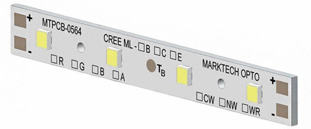
Marktech’s evaluation boards provide a solution for lighting designers and manufacturers who want to test and measure Cree Xlamps®. They help new designs get to market fast by reducing the time to prototype and characterize luminaires. Marktech offers these standard and customizable solutions, while Cree delivers the industry-leading LED technology.
Multi-Chip metal cans flexibly hold up to 7 chips of your choosing, in hermetic packaging as an alternative to 5mm ceramic stem packaging (see above).
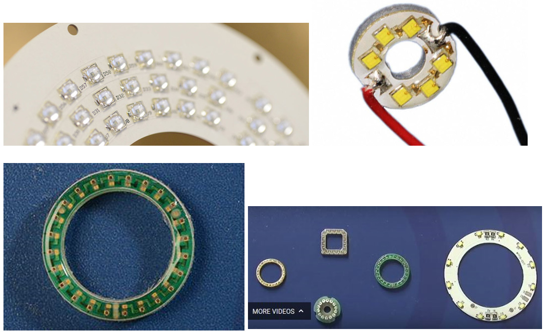
Light Rings
If your application requires high reliability and high radiant power output, but needs a compact circular footprint, a light ring may be the right LED solution for you.
Available in FR-4, metal core, and ceramic, light rings from Marktech push the boundaries in terms of chips, materials, and sizes. Marktech currently produces one of the smallest commercially available light ring for endoscopy applications at 4mm.
Additional custom designs:
If you don’t see a package that would work for your application, we can design a complete custom solution to meet your needs.
Useful references
Advanced Packaging of Optoelectronic Devices, Wiley Encyclopedia of Electrical and Electronics Engineering. Published Online: 18 JAN 2013. Copyright © 2013 John Wiley & Sons, Inc.
Epoxies for OptoElectronic Packaging; Applications and Material Properties, by Michael J. Hodgin of Epoxy Technology, Inc. Proceedings of the 36th Annual IMAPS Conference, Boston MA, Nov 17-20, 2003, pp. 26 – 30
Shining a light on LED technology, by M. Simard-Normandin of MuAnalysis
IWLPC (Wafer-Level Packaging) Conference Proceedings
Reconstituted Big-Chip LEDs on Multi-Layer Interconnects for High-Brightness Lighting. Authors: Liang Wang, Gabe Guevara, Grant Villavicencio, Roseann Alatorre, Hala Shaba, Rey Co, Eric Tosaya. Company: Invensas Corporation. Date Published: 11/11/2014 Conference: IWLPC (Wafer-Level Packaging)