The broadest line of both silicon and InGaAs detectors commercially available.
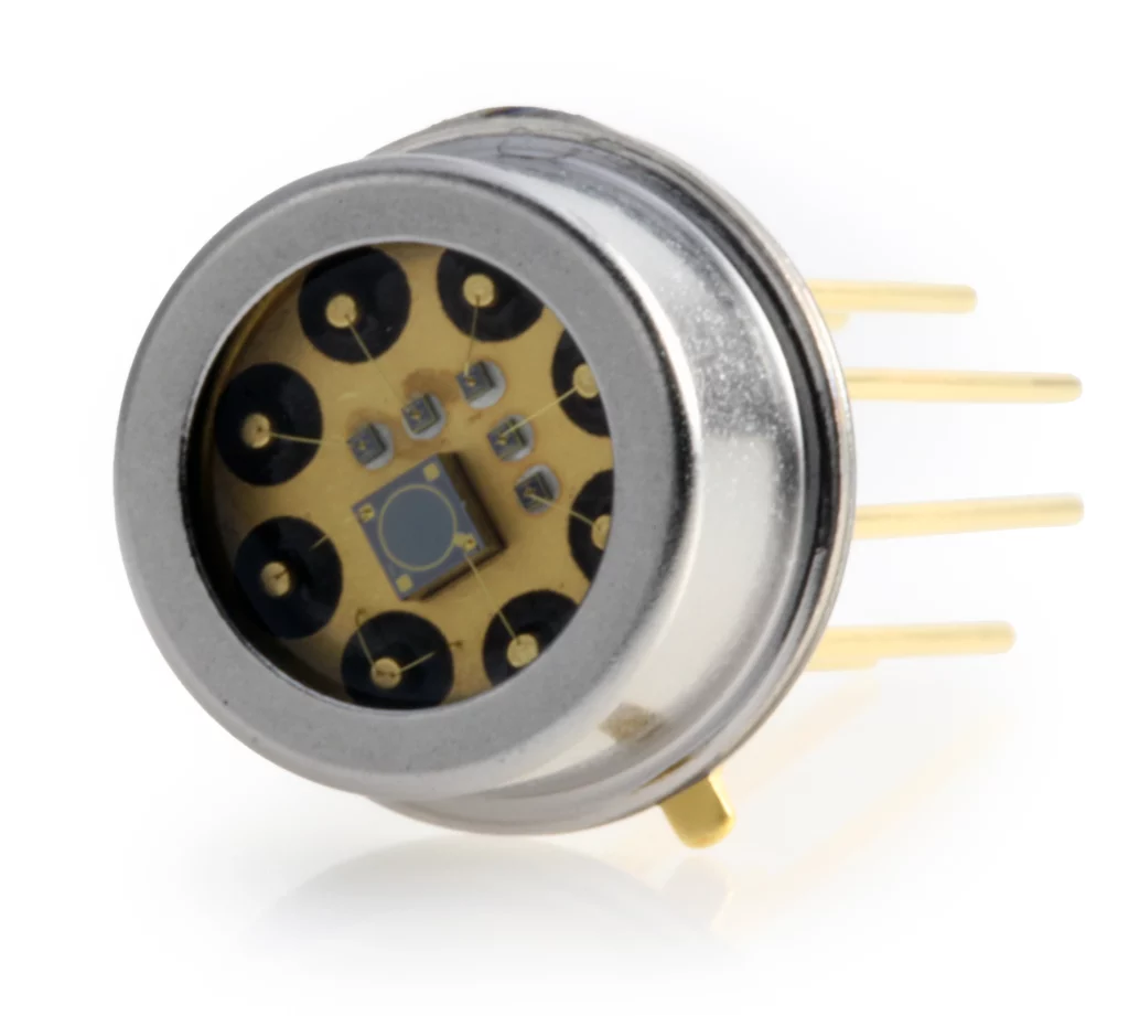
Indium Gallium Arsenide (InGaAs) PIN photodiodes are made using InGaAs/InP technology.
Cutting-edge silicon photodetectors that excel in precise detection of light ranging in wavelength from 250nm to 1100nm
Monolithic “quads” or quadrant photodiodes (QPDs) are 2 X 2 photodiode arrays with four planar diffused photodiode elements or segments.
Marktech offers a broad line of silicon photo Transistors in a variety of package types ranging from miniature metal can to ceramic packages.
Our High-Reliability Photoreflectors are sensors that contain both the LED emitter and photodetector functions within a single package.
Marktech Si APD’s offer low-level light and short pulse detections of wavelengths between 400 nm and 1100 nm.
UV detectors are offered in a variety of TO metal-can type packages from TO-18 to TO-39 with special UV glass lens to insure optimum lifetime and the least amount of material degradation
With the ability to detect light in the UV, visible, and infrared spectrums, photo detectors, photo transistors, and photodiodes are being used in increasingly more applications.
Marktech offers the broadest range of emitters commercially available ranging from 235nm to 4300nm across the UV, visible, NIR, SWIR, and MWIR spectral ranges.
Marktech offers the broadest range of UV LEDs commercially available ranging from 235nm to 400nm including UVA, UVB, UVC, and deep UVC LEDs.
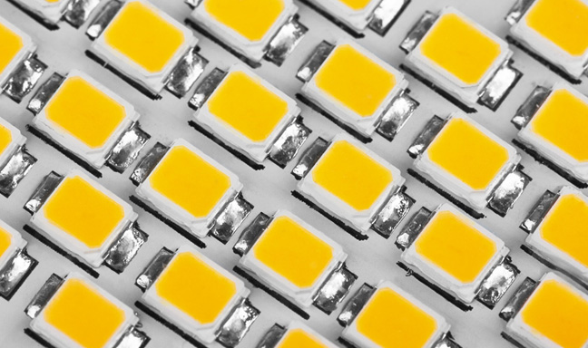
Our advanced line of visible LED products is engineered to deliver high-quality, energy-efficient lighting solutions across various applications from 400nm to 700nm..
Our NIR LED wavelength range is typically from 700nm to 1000nm, extending into wavelengths invisible to the human eye but crucial for numerous technological and scientific applications.
Our standard product offering includes wavelengths from 1020nm to 4300nm and operating currents ranging from 20mA to 350mA for high-power applications.
Our Point Source LEDs are specifically engineered for optical encoders, edge sensors, and other critical applications that demand highly focused light with minimal dispersion.
Multi-LED chips in a single package, our multiple wavelength LEDs are engineered to address a myriad of applications across the UV, visible, NIR, SWIR, and MWIR spectral ranges
Designed to produce a highly defined red dot or reticle, facilitating accurate aiming without revealing the location to the target.
Ideally suited for applications including edge sensing, line sensing, coin bill validation, and bar code reading
Our panels are crafted to deliver uniform, vibrant illumination across a wide range of applications, from consumer electronics to industrial displays.
Crafted with the latest LED technology, these rings provide adjustable illumination to meet specific needs, ensuring optimal visibility and enhancing the quality of your projects.
As a proud CREE LED Solution Provider for over a decade, Marktech offers comprehensive engineering support, including design, binning, and material selection, alongside custom packaging options for specialized applications.
CREE LED through-hole emitters, designed for high-temperature and moisture environments with UV-resistant optical-grade epoxy, offer a range of colors for versatile applications in signage and lighting.
CREE High Brightness (HB) SMD LEDs are the brightest, most reliable architectural, video, signage, scoreboard, roadway, and specialty LEDs available today.
CREE LED’s P4 series represents a leap in LED design, combining efficiency with aesthetic versatility to meet the demands of modern lighting applications.
Marktech’s CREE LED XLamp® offerings on aluminum core starboards simplify LED integration for designers, providing a range of colors and angles on compact boards for easy testing and implementation in varied lighting applications.
Marktech Optoelectronics introduces its new product line of CREE LED die, including the EZ1350 Series Die, packaged in TO-cans (TO-18 and TO-39 outlines) designed for precision and reliability in demanding applications with protection against environmental factors like moisture and dust.
CREE LED’s Versatile InGaN-based LED chips are designed to meet diverse needs for blue, green, and white-converted LEDs.
Marktech Optoelectronics combines over 40 years of expertise in optoelectronics with a focus on customized engineering solutions, addressing specific customer needs and applications.
Custom photodiode detectors are designed to meet unique customer requirements, offering specialized performance features and cost savings through optimizations such as integrated filters, photodiode arrays, and hybridization.
Through our vertically integrated manufacturing facilities in California and Japan, we offer custom LED solutions, including packaging and optoelectrical categorization, enhancing product design and market readiness.
Multiple LED dies combined in a single package are engineered to address various applications across the UV, visible, NIR, SWIR, and MWIR spectral ranges.
To succeed, you need the exact optoelectronic package custom-designed and manufactured for your application, including hermetic metal SMD, TO-can, plastic SMD, and molded through-hole packaging.
Made-to-order semiconductor chips (die) and wafers are designed and fabricated to fit your needs. Standard dies are available in specific wavelengths for high-volume production applications.
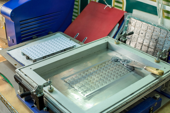
Bare and encapsulated LEDs, photodiodes, and other components are assembled on FR4, metal-cored, and flexible circuit boards, ready for production.
Learn about the latest trends, devices, and potential applications.
The latest news and announcements from Marktech Optoelectronics.
Detailed information about common uses for Marktech Optoelectronics devices.
In depth discussions on LEDs, Detectors and the science behind them.
Become familiar with common terminology and concepts for LED Devices.
List of common concepts and definitions for Photodiodes.


