
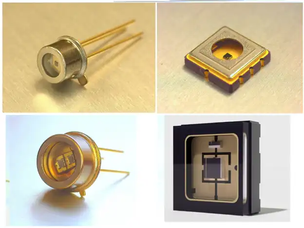
Marktech’s NEWEST Photodiodes and LEDs – Now Available on DigiKey

Marktech Optoelectronics announces the release of its latest optoelectronic components—now in stock at DigiKey. The updated lineup includes UV, visible, NIR, and SWIR LEDs, along with advanced photodiodes for demanding detection applications. Designed for precision sensing and emission tasks, these components serve medical, industrial, aerospace, and environmental markets. Solar-blind SiC detectors with increased active area […]
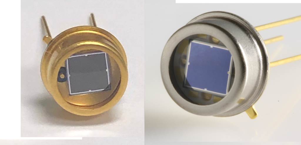
Don’t Pay Up to 145% More for Silicon Photodiodes — Buy Marktech Si PDs Designed, Fabricated, and Assembled in the U.S.A.
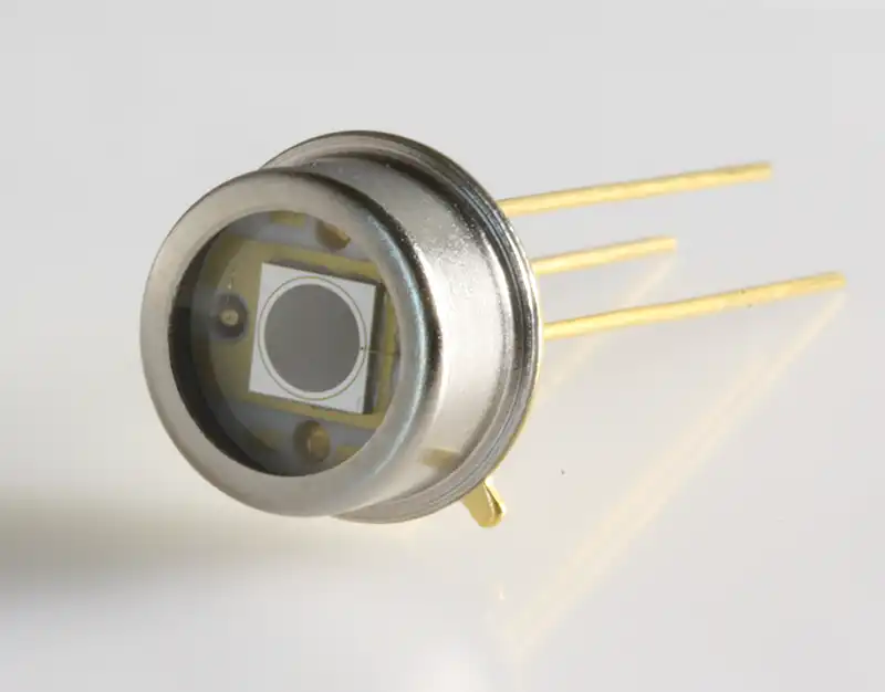
In today’s competitive component marketplace, price and performance both matter. That’s why Marktech Optoelectronics is making a clear call to OEMs, integrators, and system designers: don’t overpay for silicon photodiodes. Marktech’s high-performance silicon photodetectors are designed, fabricated, and assembled entirely in the United States—often at up to 145% lower cost than imported or private-labeled alternatives. […]
Marktech’s latest MWIR LEDs support Precision MWIR Applications
Marktech’s MWIR LEDs with peak wavelengths of 3100nm, 3700nm, 3900nm, 4100nm, and 4300nm Marktech Optoelectronics Inc. is pleased to announce a webinar on “InGaAs Photodiode Detectors: Packaging, Performance, and SWIR Applications”, presented by Vince Forte, the company’s Chief Technology Officer. The webinar will be pre-recorded and will be available for viewing starting May 10th through […]
Explore Our Innovations at PHOTONICS WEST 2025
If you are attending PHOTONICS WEST 2025 in January, stop by our booth (#237) from 28 to 30 January 2025 in San Francisco. Photonics West is the leading event worldwide that showcases the latest products from electro-optical and optical technology industry leaders worldwide. Marktech is co-exhibiting at Photonics West 2025 with two of our esteemed […]
Marktech’s CTO, Vince Forte, Presents on Multi-chip Emitter-Detectors at the Photonics Media Sensors and Detectors Summit
If you are attending the online Photonic Media’s Sensors and Detectors Summit on Wednesday November 13th, 2024, please listen to the presentation, “Multi-Chip Detector-Emitter Packages and Their Applications” delivered by our Chief Technology Officer, Vince Forte. The summit highlights breakthroughs and exciting new optoelectronics technologies impacting the sensors and detectors industry worldwide. https://events.photonics.com/Event.aspx?EID=25&OC=OM Vince’s presentation […]
Marktech Optoelectronics Brings Cutting-Edge UVC LEDs, Photodiodes, and IR Emitters to Electronica 2024
If you are attending electronica 2024 from November 12th to 15th, please stop by our booth (C5/521) at the Messe München Exhibition Center in Munich, Germany. The electronica show highlights breakthroughs and exciting new products in electronics from manufacturers worldwide. (visit https://electronica.de/en/trade-fair/) Marktech Optoelectronics will be displaying both their well-established and newly released products and […]
See Us at NYS Innovation Summit 2024
If you are attending the New York State Innovation Summit 2024 on October 28th and 29th, please stop by our booth (#408) at the ON Center in Syracuse, NY. The NYS Innovation Summits highlights the major breakthroughs and exciting new products produced by New York State manufacturers. Deep UVC LEDs and Solar Blind SiC […]
See Us at Sensor Expo Japan 2024

If you are attending SENSOR EXPO JAPAN 2024 in September, stop by our booth (#S-20) from September 18th to 20th at the Tokyo Big Sight East Hall 2 in Tokyo, Japan. SENSOR EXPO JAPAN is a world-renowned event that showcases the latest products from sensing technology industry leaders around the world. Marktech is co-exhibiting at […]
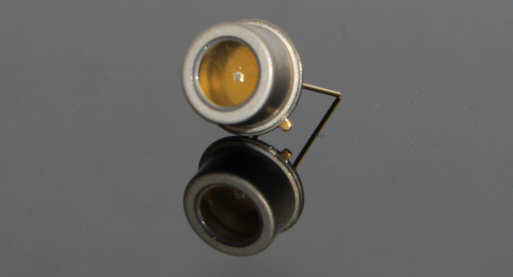
Marktech Releases New Low Capacitance, High-Speed Silicon Photodiodes – 3X Response Speed
Latham, NY – August 28, 2024 – Marktech Optoelectronics, a leading innovator in optoelectronic components, proudly announces the release of its new line of low-capacitance, high-speed silicon photodiodes. These advanced photodiodes are designed to meet the demanding requirements of high-speed optical systems, offering unparalleled performance in various applications. The new Series 4 silicon photodiodes have […]
Marktech Optoelectronics Launches Advanced Silicon Carbide (SiC) Photodiodes for Deep UVC Detection
[Latham, NY, July 24, 2024]—Marktech Optoelectronics, a leader in optoelectronic technologies, is proud to introduce its latest innovation: Silicon Carbide (SiC) photodiodes designed for deep UVC detection. These photodiodes exhibit visible light or solar blind characteristics, making them ideal for monitoring 235nm and 255nm far or deep UVC LEDs. [Latham, NY, July 24, 2024]—Marktech Optoelectronics, […]