
Marktech Optoelectronics Launches Advanced 235nm and 255nm UVC LEDs on Starboards
Marktech Optoelectronics, a leader in innovative light emission and detection solutions, today announces the launch of its new 235nm and 255nm UVC LEDs mounted on starboards, a significant innovation designed to accelerate the development and prototyping of sensors, instruments, and sanitizers. These state-of-the-art UVC LEDs on starboards are a convenient solution, relieving optical and electrical […]
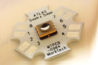
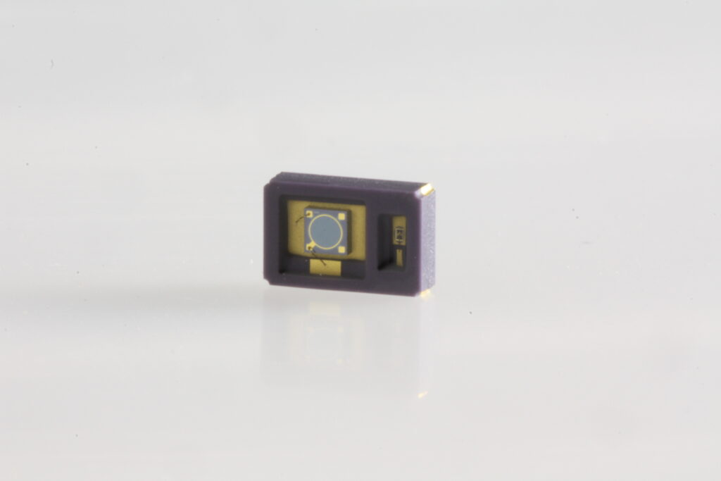
Marktech Expands their Multi-chip Product Line with Multi-Wavelength SWIR LEDs and a 2.6µm InGaAs Detector in One Package
Marktech MTMD34679PD6T38 – SWIR multi-chip emitter-detector with multiple wavelength LEDs April 23, 2024 – Latham, NY, USA – Marktech Optoelectronics, Inc. (www.marktechopto.com)(Marktech), a privately-held leading designer and manufacturer of standard and custom optoelectronics, including UV, visible, near-infrared (NIR), and short-wavelength infrared (SWIR) emitters, detectors, InP epi wafers, and other compound semiconductors, today reveals their new […]
Maximize Your Total Cost Benefit with Tailored Photodiodes and LEDs for OEM Designs

Photodiodes and LEDs are widely used in a range of applications, including optical sensors, communication systems, medical diagnostic devices, analytical instruments, and application specific lighting. They are often used together to maximize the total cost benefit, with photodiodes serving as detectors and LEDs as emitters. By tailoring these components to OEM design needs, engineers can […]
Marktech Optoelectronics Releases New Green and Red Dot LEDs – Just in Time for the Holidays
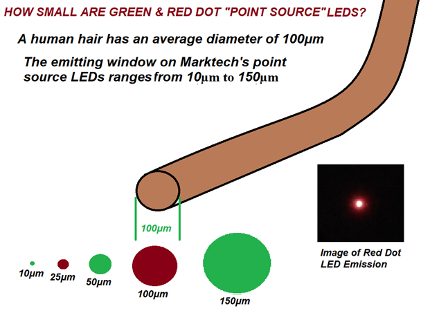
Marktech’s Introduces Standard Green Dot LEDs and Expands Red Dot LED Line-up Marktech Optoelectronics, Inc. (www.marktechopto.com)(Marktech), a privately-held leading designer and manufacturer of standard and custom optoelectronics, including UV, visible, near-infrared (NIR), and short-wavelength infrared (SWIR) emitters, detectors, InP epi wafers, and other compound semiconductors, today announced the release of their enhanced sharpness 25 and […]
Buying Your Engineer or Scientist a New Photodiode for Christmas? 8 Questions to Ask When Selecting A Photodetector Manufacturer
1. How extensive is the photodiode manufacturer’s product offering? Do their photodiodes have the wavelength sensitivity, speed, active area, and other performance parameters to meet your photo- detection requirements? The supplier should have a broad enough product line to meet your current and future needs. They should have photodiodes in their line-up meeting your application’s […]
Marktech Optoelectronics Announces the Launch of Innovative Quadrant Silicon Photodiode – MT03-072
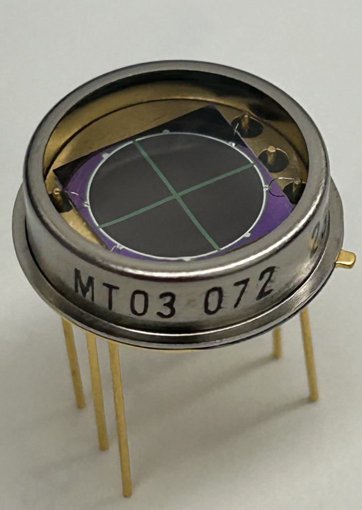
[Latham, NY, November 28, 2023] – Marktech Optoelectronics, a renowned leader in optoelectronic components, is excited to announce the release of its latest innovation, the Quadrant Silicon Photodiode, part number MT03-072. This state-of-the-art photodiode meets the advanced needs of applications such as beam centering, beam nulling, position centering, beam alignment, optical tweezers, atomic force microscopes […]
Advanced 235nm and 255nm UVC LEDs: The Future of Germicidal UV Solutions
Marktech Optoelectronics Launches Advanced 235nm and 255nm UVC LEDs:The Future of Germicidal UV Solutions [Latham, NY, November 14,2023] – Marktech Optoelectronics, a leader in innovative light emission and detection solutions, proudly announces the release of cutting-edge 235nm and 255nm UVC LEDs from Silanna housed in flat and dome lens SMD and TO-cans packages (e.g., MTE2350F-UV and MTE2350D-UV). This […]
Register for Our Webinar – InGaAs Photodiode Detectors: Packaging, Performance, and SWIR Applications – May 10th 2023

Register for Our Webinar – InGaAs Photodiode Detectors: Packaging, Performance, and SWIR Applications – May 10th 2023 Marktech Optoelectronics Inc. is pleased to announce a webinar on “InGaAs Photodiode Detectors: Packaging, Performance, and SWIR Applications”, presented by Vince Forte, the company’s Chief Technology Officer. The webinar will be pre-recorded and will be available for viewing […]
Marktech Expands Surface Mount SWIR Reflective Sensor Offerings
October 2, 2019 – Latham, NY, USA – Marktech Optoelectronics, Inc. (www.marktechopto.com)(Marktech), a privately-held, VOSB-certified, leading designer and manufacturer of standard and custom optoelectronics components and assemblies, including UV, visible, near-infrared, and short-wave infrared (SWIR) emitters, detectors, InP epiwafers, and other materials, today announced the recent expansion of its industry-exclusive surface mount (SMD) SWIR reflective […]
Marktech Expands Standard Silicon Photodiode Offerings to Include New Processes, Active Area Sizes, Case Isolation, and Package Options
August 12, 2019 – Latham, NY, USA – Marktech Optoelectronics, Inc. (Marktech), a privately-held, VOSB-certified, leading designer and manufacturer of standard and custom optoelectronics components and assemblies, including UV, visible, near-infrared (NIR), and short-wave infrared (SWIR) emitters, detectors, InP epiwafers, and other materials, has expanded its standard Silicon photodiode offerings to include additional processes, active […]