Skip to content

LED Component and Assembly Miniturization

The trend towards miniaturization in the electronics world is on-going and is fueled by a variety of factors including the consumer’s desire for portability as well as improved efficiency and reductions in costs. Over the past few years, LED (Light Emitting Diode) technology specifically, has seen tremendous growth, primarily due to the revolution in the lighting and general illumination markets. This increased interest in LEDs has also extended to a variety of other markets including military, medical and machine vision. Although LEDs are not new to these markets, their demand for smaller, higher resolution and uniform sources continues to grow. Essentially there are three basic categories of components in the LED environment. These are Through-Hole, Surface Mount and COB (Chip-On-Board). We will review these to help understand the miniaturization process regarding the design and use of LEDs for applications in these markets. Through-hole LEDs have been commercially available since the 1960s. They come in a variety of body types but typically range in size from 3mm – 10mm in diameter (See figure 1).

FIGURE (1)

These devices dominated the optoelectronics and technology sectors for more than 20 years. They are still widely used today in a variety of applications ranging from large digital displays and VMS (Variable Message Signs) to standard indicators for consumer or industrial electronics. Although these LED types are larger in size compared to the latest technological developments, there are still advantages to using through-hole devices such as integrated optics, ease of manufacturing and low cost. In addition, many display or VMS type applications do not require high resolution graphics or extensive color mixing for full color viewing. It wasn’t until the 1980s and 90s when the cell phone and computer industries began their rapid escalation into the homes of every consumer, that the push for miniaturization commenced. Surface mount components, although actually developed in the 1960s, were rapidly replacing through-hole devices beginning in the late 1980s. This technology not only allowed for much higher circuit densities, thus significantly reducing size, but it also made automated assembly possible. Hand soldering became less and less necessary. Surface Mount Devices allowed for the mounting of components on both sides of the PCB or Printed Circuit Board as opposed to only one side. (See Figures 2A – 2B) Figure (2A) – Through-Hole Front Side Populated, Back Side – soldering only, no components Figure (2B) – Surface Mount Components on front and back of PCB This in-turn had other advantages which included reduced manufacturing costs, improved thermal properties, increased reliability and faster turn-around time of assemblies. In addition, it was then possible to create high resolution displays as well as full color variable message signs utilizing red, green and blue LEDs. Blue LEDs also became commercially viable in the 1990s coinciding very well with the wide use of surface mount components. Surface mount devices have today become the product category of choice for most electronic design applications and come in a variety of package types and sizes. Some of the most common in the LED world range in size from 0402 which equates to .04″ x .02″, to 1210 or .12″ x .10″ with larger sizes for high powered devices. (See figure 3)

FIGURE (3)

In the late 2000’s, a push for even greater efficiency and increased density for LEDs was occurring, once again, primarily driven by the lighting and general illumination market. This resulted in the widespread introduction and usage of COB (Chip-On-Board) technology. COB is a semiconductor technology where the “chip” also referred to as the “die” is mounted directly on the printed circuit board using a procedure called die attach or die bonding. The individual die are placed on the PCB by either using a conductive paste or soldering (Eutectic) method and then wire bonded. (See figure 4) This technology virtually eliminates the need for additional packaging such as lead frames and housings which allows for greater thermal dissipative qualities, reduced size and increased LED density (if required).

FIGURE (4)

140pcs of a LED chip packaged into an area less than 1 square inch There are still challenges with using COB technology especially from a manufacturing standpoint. Some of these include; (A) Capital expense – The equipment required is often very specialized and expensive (B) Uniformity and consistency is critical in many COB applications, therefore, the bare Die / Chip must be carefully selected and tested prior to placement on the PCB. This process also requires very specialized equipment and in addition, the yields must be considered to maintain a cost effective device. (C) Re-Work of COB assemblies can be difficult if already encapsulated. In some cases, the entire product must be discarded. If the product is able to be re-worked, typically, it can only be performed at the factory. Conversely, if the device is not encapsulated, re-work is relatively easy to perform compared to through-hole and SMT technology and less costly. (D) The quality, uniformity and type of PCB is critical to insure proper die attach and wire bond integrity. Pure, wire-bondable gold is often required. COB technology is now being used by almost every major LED manufacturer, primarily in the general illumination and lighting marketplace. The increasing demand for energy efficient solutions to incandescent, halogen and similar antiquated technologies is allowing for rapid growth in the COB LED arena. As this technology continues to improve and costs decrease, the COB LED assembly market is expected to exceed the overall standard LED market in the next several years. Although most manufacturers are focused on energy efficient solutions to general illumination, there are a few select LED manufacturers who are using the many advantages of COB technology in more niche, highly specialized applications such as military, medical, machine vision and security. An offshoot of COB technology which further increases efficiency and provides an even greater opportunity for miniaturization are the Direct Attach and Flip Chip methods of assembly. Both methods do not require wire bonding thus allowing for a lower profile COB assembly while improving performance. Currently, a limited number of LED manufactures are providing this type of die structure. In addition, there are even a smaller number of assemblers that are capable of properly mounting this type of die. A major supplier of DA die is Cree, Inc. An example of one of their DA type chips is shown in figure 5.

Figure (5) DA top and bottom view

The Direct Attach technique uses a flux eutectic bonding process which eliminates the need for solder paste, preforms or conductive adhesives. An appropriate flux and PCB is all that is required to achieve a high quality bond during the re-flow process. An example of an assembly made with standard COB technology versus DA bonding is shown in figures 6A – 6B.

Figure (6A) Standard COB assembly (Wire Bonding Required)

Figure (6B) Direct Attach assembly (No Wire Bonding Required)

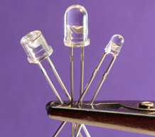
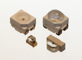
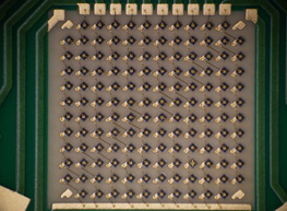
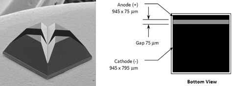
Flip chip technology flips over the LED in a face down orientation and places the electrodes in direct contact with the PCB. Like the Direct Attach process, this technology gives LED chips advantages that include a larger light-emitting area, better heat dissipation, along with eliminating the wire-bonding step and wire bond shadowing. The bonding method for flip chip die uses what are called solder “bumps”. The attachment process consists of applying the appropriate type of flux (as in the DA method) to these solder bump areas and then performing a reflow process. Due to the CTE (Coefficient of Thermal Expansion) mismatch between the flip chip and PCB, it is typically not recommended to use FR-4 material but a ceramic or optimized MC (Metal Core) substrate PCB. A major supplier of flip chip type die is Philips LumiLED. (See Figure 7)
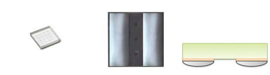
Figure (7) Flip Chip top view, bottom view and side view w/solder bumps

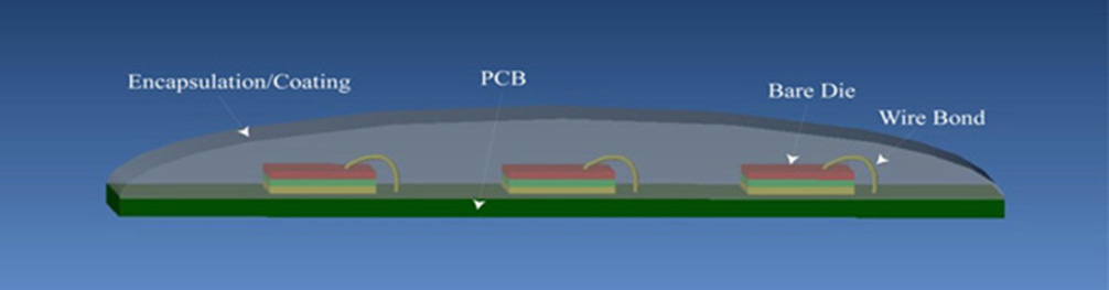
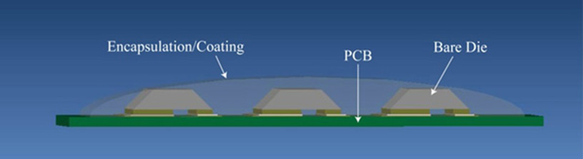
Both of these technologies are relatively new to LEDs but are beginning to make large inroads into the general illumination and niche marketplaces mentioned previously. In addition to some of the advantages described earlier, the reduction in thermal resistance going from a through-hole device to COB (see figure 8) will result in significant improvements in the lifetime and performance of the product.
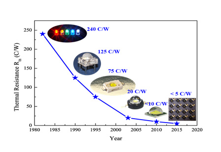
Figure (8) Thermal Resistance Comparison (Junction to Pad)

As with any new technology, it is critical to insure you are working with an organization that is experienced in optoelectronics, is aware of the advantages and disadvantages of through-hole, SMT or COB and is capable of providing the best option for your application. Vincent is Chief Technology Officer of Marktech Optoelectronics in Latham, New York. He has been in the optoelectronics field for nearly 30 years and has authored or co-authored several articles relating to LED technology. Many significant enhancements to LEDs and their applications have directly resulted from Vincent’s input and hands-on experience.

View Products

Find something you were looking for? Get a free no-obligation quote today.