Buy Now

Buy Now

Buy Now

Need parts?

Buy Now

Marktech Releases Higher Power UV LEDs for Disinfection, Curing, and Sensing — Now Covering 230 to 340nm

Industry-Leading UV LEDs Enabling New Designs for Curing, Sensing, and UVGI Disinfection Systems

Latham, NY — December 17, 2025 – Marktech Optoelectronics (“Marktech”), a leader in advanced UV LED and ultraviolet LED emitter technologies, today announced an expanded portfolio of high-power UV LED light sources with new UV emitters spanning 230nm to 340nm. These devices strengthen Marktech’s offerings across the ultraviolet light spectrum—from deep-UV LED (DUV LED, far UVC LED) sterilization wavelengths to longer UVB and UVA wavelengths for curing, phototherapy, and forensics.


Image opf Deep UVC 235nm LED mounted on a metal-cored starboard for rapid prototype and design evaluation.
Deep UVC 235nm LED mounted on a metal-cored starboard for rapid prototype and design evaluation.

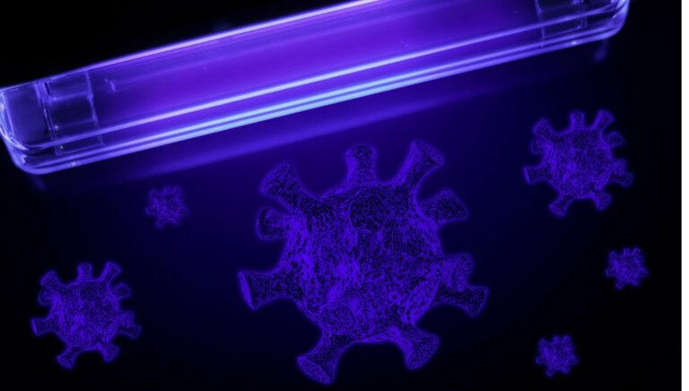
These next-generation emitters meet the growing demand for UV sanitizing light, germicidal UV light (UVGI light), UV curing light, LED light curing, deep UV sterilization, phototherapy (psoriasis, eczema, vitiligo, and acne treatment), PUVA therapy (enhanced UVA phototherapy using psoralens light-sensitizing compound), fluorescence excitation, spectroscopy, 3D-printing resins, water quality monitoring, medical UV light, UV water disinfection, and precision sensing applications.

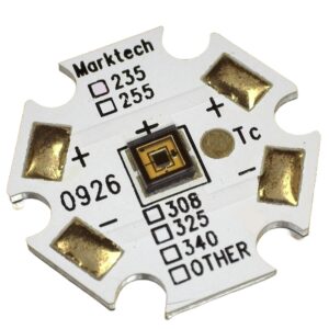
The updated UV product family adds new deep UV (230nm and 265nm), UVB (310nm), and UVA (340nm) parts while maintaining Marktech’s hallmark of reliability and precision. Each device is engineered for high output and narrow spectral bandwidths. Custom multi-chip configurations, matched emitter‑- detector pairs, and starboard versions are available.

High-Power 280nm LEDs, available in single- and four-chip versions, in SMD and SMD-scaled chip-on-substrate (COS) formats, will follow in early 2026. Marktech and our partners continue to innovate and expand our UV LED offerings into the far-UVC spectral range for sensing, chemical analysis, and ultraviolet germicidal irradiation (UVGI) applications.

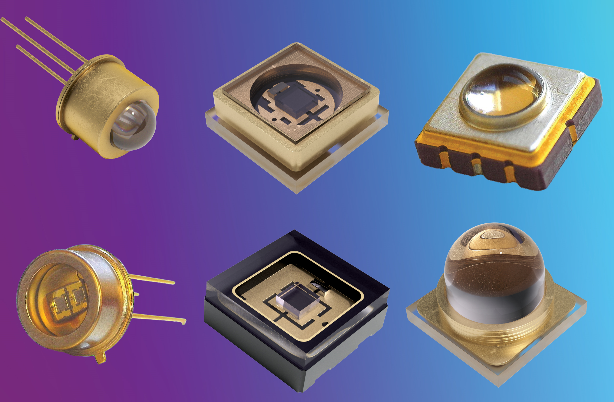
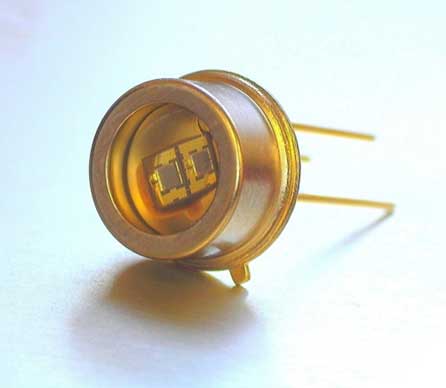
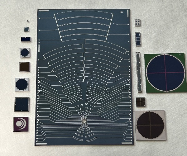
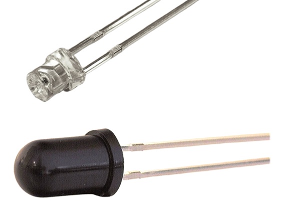
The updated product family includes UV LED chips or UV LED dies in a variety of packages:

  • Metal-can UV LEDs (UVC LEDs, UVB LEDs, high-power UVA LEDs)
  • SMD UV LEDs, including our proprietary hermetic ATLAS SMD package
  • Chip-on-board or COB UV LEDs
  • 5mm and 3mm molded through-hole UVA LEDs (> 350nm)
  • Compact, low-profile transfer-molded UVA LEDs (> 350nm) (Coming in 2026)

Note: Note all wavelengths are available off-the-shelf in all package types, but custom packages can be developed to meet your OEM design needs.

The range of wavelengths in Marktech’s expanded UV LED lineup now includes:
405nm (near UV), 400nm, 395nm, 385nm, 375nm, 370nm, 365nm, 355nm, 340nm, 325nm, 310nm, 295nm, 285nm, 275nm, 265nm, 235nm, 255nm

Images of various UVC LEDs in several different package types. Examples of Marktech's deep UVC LEDs (235nm, 255nm), which were recognized as a finalist in Cleantech / Sustainability category of Best of Sensors 2024 competition

Examples of Marktech UV LEDs in the UVC and UVB spectral ranges.

Applications Across Multiple Markets (with Peak Wavelength Guidance)

  • Medical & laboratory disinfection equipment (230–280 nm, 315-400nm) – Ultraviolet germicidal irradiation for surface, instrument, and airborne sterilization.  the optimum UVC LED peak for destroying a pathogenic microbe can vary depend on the specific family and species of pathogen (live bacteria, fungi, protozoa, virus, and dormant spores), the lifetime and degradation of UVC LED output over time, and the transmission through or absorption by the microbes and media containing the microbial mass.
    • 255nm and 235nm UVC LEDs – Wound disinfection at 235 nm looks promising for healing recalcitrant or chronic wounds when an infection or bacterial biofilm inhibits normal healing. Ultraviolet wavelengths below approximately 240 nm cause less damage to human tissue (skin and eyes) than 265nm and 280nm, but further studies are needed to confirm this. Also, the lower power output and lifetime of UV LEDs below 240nm limit sanitization effectiveness. Marktech is addressing some of these issues with new 2X-higher-power ~230 nm UVC LED chips compared to earlier products. In addition, we have manufactured deep UVC LEDs with multiple 235nm chips in a single package to increase power output further.
    • 265nm is the absorption peak for DNA, and destruction of DNA is typically seen as the best way to inactivate or kill pathogens, as long as the power output is sufficient, and can be maintained over the lifetime of the product. In addition, the
    • 280nm is the absorption peak for protein, which provides another route for destroying harmful microbes. While not as effective as 265nm or smaller UVC LED wavelengths in a head-to-head comparison at the same power output and transmission rates, many manufacturers are moving toward UVGI systems using 280nm UVC LEDs due to the higher power output and wall plug efficiency (WPE) media
    • Multiple UV Peak Wavelength Combinations – The 265nm+280nm and the 230nm+265nm+280nm peak UV wavelength combinations could potentially provide even higher effectiveness than using a single peak wavelength UVC LED. Multiple-wavelength UVC light can exhibit synergistic effects, leading to faster inactivation and greater energy efficiency. Marktech can package multiple UV LEDs with different peak wavelengths in a single package. For instance, we could custom package four 230nm UVC LEDs with one 265nm UVC LED and one 280nm UVC LED. A 265nm+280nm LED with addressable chips is useful device for DNA purity analysis.
    • 315 to 400nm UVA LEDs combined with a titanium dioxide (TiO2, titania) photocatalyst can be used to generate highly reactive oxygen (ROS) with the ability to eradicate microorganisms. Another disinfecting gas, ozone, can be generated using deep UVC wavelengths at 200nm or shorter. Ozone, ROS, and ethylene are effective for disinfecting surgical instruments and medical devices, but they are also toxic to humans.
  • Phototherapy or photobiomodulation
    • 310nm UV light exposure is commonly used to phototherapy for psoriasis, eczema, vitiligo, and acne treatment.
    • 365 nm psoralen UVA (PUVA) therapy (enhanced UVA phototherapy using psoralen light-sensitizing compound). 8-methoxypsoralen (8-MOP) interacts with DNA enhancing UVA light absorption.
  • Water & air treatment (230–280 nm) – UV‑C wavelengths optimized for microbial and viral inactivation.
  • 3D printing & photopolymer curing (365 nm) – UV‑A curing for resins, coatings and adhesives.
  • Fluorescence, spectroscopy & chemical sensing (250–405 nm) – 260–280 nm for protein/nucleic‑acid excitation; 310–340 nm for aromatic compounds and minerals; 340–365 nm for scattering-based detection. By comparing the absorption at 265nm to the adsorption at 280nm the level of protein remaining in a DNA sample can be assessed. Dual addressable 265nm+280nm LEDs with additional optical filters can be helpful measuring protein or DNA purity.
  • Water quality analysis – Water quality instruments leverage several deep UVC wavelengths for chemical oxygen demand (COD), dissolved organic matter (DOM), biological oxygen demand (BOD), and total organic carbon (TOC).

    Parameter

    Primary UV Peak (nm)

    Measurement Type

    Notes

    Organic Matter / DOM

    254 nm (255nm)

    Surrogate

    Aromatic organics

    COD (UV method)

    254 nm (255nm)

    Correlative

    Site-specific calibration

    BOD (UV proxy)

    254 / 280 nm

    Model-based

    Not direct

    TOC / % Organic

    205–215 / 254 nm or 220nm+235nm+255nm

    Correlative

    Needs calibration

          Nitrate (NO₃⁻)

    220nm+254nm,
    235nm+280nm

    Direct Absorbance

    255nm, 280nm for organic correction
     

  • NDT inspection & UV‑A illumination (340–370nm, typically 365nm) – Industry‑standard wavelengths (~365nm) for penetrant inspection, forensic analysis, leak detection, and QA/QC.
  • Security marking & authentication (340–405 nm) – Covert UV‑reactive inks and anti-counterfeiting materials in currency, documents, and critical products.
  • Forensics (300405nm, mainly 365nm & 395nm, 255nm for RUVIS)  – 365nm UVA LED light sources are typically employed to detect biologicals and trace evidence such as blood, hair, semen, latent prints, and urine. 395 to 425 (near-UV to blue) peak wavelength LEDs are helpful in document examination and the identification of specific fibers. Reflected Ultraviolet Imaging Systems (RUVISs) illuminate surfaces with 255 nm or 254nm light to reveal latent fingerprints, often without the need for powders or chemicals such as cyanoacrylate fumes. RUVIS can also reveal hidden bruises, especially on dark skin, by exploiting differences in light absorption/reflection from blood pigments.

Product Table – Peak Wavelengths, Power, and Viewing Angle. Datasheets & Buy Now Links

Part Number

Peak λ (nm)

Angle
 (
°)

Power (nW)

Datasheet

Buy Now

Buy Now

Digi‑Key

Mouser

MTE2550KC9‑UV

255nm

10

0.8

PDF

Digikey

Mouser

MTE2550KCL9‑UV

255nm

115

1.8

PDF

Digikey

Mouser

MTE2650KC9‑UV

265nm

10

1.2

PDF

Digikey

Mouser

MTE2650KCL9‑UV

265nm

115

1.9

PDF

Digikey

Mouser

MTSM310UV‑F1120

310 nm

120

1.2

PDF

Digikey

Mouser

MTSM310UV‑F1120S

310nm (Starboard)

120

1.2

PDF

Digikey

Mouser

MTSM340UV‑F3120

340 nm

120

90

PDF

Digikey

Mouser

MTSM340UV‑F3120S

340nm (Starboard)

120

90

PDF

Digikey

Mouser

MTSM340UV‑D3065

340 nm

70

85

PDF

Digikey

Mouser

MTSM340UV‑D3065S

340nm (Starboard)

70

85

PDF

Digikey

Mouser

MTSM340UV‑D3035

340 nm

35

80

PDF

Digikey

Mouser

MTSM340UV‑D3035S

340nm (Starboard)

35

80

PDF

Digikey

Mouser

Note: For starboard (“S”) versions, the electrical and optical characteristics are identical to their base part numbers. The star‑board option provides UV LEDs pre-mounted on a metal-cored PCB for faster evaluation and easier integration into prototype designs. This eliminates the need for a design engineer or electronics designer to develop and build a custom circuit board.

High Reliability Design


Marktech’s new emitters combine advanced semiconductor materials with optimized thermal paths and durable package designs. In the deep‑UV MTE2550/MTE2650 series, peak wavelengths of 255 nm and 265 nm are achieved with narrow spectral bandwidths and sealed metal‑can packages. The MTSM310UV series features a ceramic surface-mount design with low thermal resistance and a peak emission at 310 nm, making it suitable for biochemical sensing and phototherapy applications. The MTSM340UV family delivers higher radiant flux at 340 nm in compact 3.5 × 3.5 mm SMD packages and is available in both base and star‑board formats.

All devices are rated for high reliability and extended lifetime under continuous drive. Custom wavelength selections, multi-chip arrays, and emitter–detector matched pairs are available on request.

UVC Safety and Compliance for OEMs

Using UVC as a “cure-all sanitizer” without accounting for efficacy, safety standards, exposure limits, regulatory constraints, and proper engineering controls is risky.  Any UVC‑based product, whether for air disinfection, surface sterilization, water purification, medical device sanitization, or OEM integration, must therefore be carefully specified, tested and labelled to ensure both efficacy and compliance with safety standards.

Read our tech brief on UVC Safety and Compliance for OEMs here:
https://marktechopto.com/uvc-safety-and-compliance-for-oems/

Availability and Ordering

Our UV LEDs are available now through Marktech and its authorized distributors. Samples and production quantities can be ordered immediately via DigiKey or Mouser using the links in the table above. High-power 235nm, 255nm, and 280 nm UVC LED devices are under development and will be released in 2026 to expand Marktech’s germicidal UVC lineup.

For technical support, custom packages, and Silicon photodiode or SiC UV detector pairings, please contact:

Marktech’s global network of distribution partners also supports application engineering, ordering and logistical needs in North America, Europe, and Asia.


Visit Our Booth at Photonics West 2026 to Learn More About Our Photonics Silicon Photodiode Manufacturing Capabilities

Plan now to visit our booth (#259) at SPIE Photonics West, 17 – 22 January 2026 in San Francisco, California to help us celebrate 40 years of photonics innovation.
SPIE Photonics West is the optics and photonics industry’s flagship exhibition to meet the sector’s biggest names and learn about the latest innovations.

Learn more: https://spie.org/PW

See our PW26 company listing: (https://spie.org/ExhibitorDetail?ExpoID=5022&ExhibitorID=104424)


About Marktech Optoelectronics

Founded in 1985, Marktech Optoelectronics, Inc. (www.marktechopto.com) (Marktech) is a privately held joint venture of Optrans Corporation and Marktech International. Marktech is a top designer, low-volume packager, and fabless manufacturer of silicon photodiodes, as well as a value-added distributor of custom optoelectronics, including UV, visible, near-infrared (NIR), and short-wavelength infrared (SWIR) emitters, MWIR LEDs, detectors, InP epi wafers, and other compound semiconductors. Headquartered in Latham, NY, Marktech operates extensive optical and electrical testing laboratories for full characterization of detectors and emitters and pioneered tight sorting for LED peak wavelength and output power—still essential for many medical diagnostic applications.
https://marktechopto.com/

About Optrans Corporation

Optrans Corp. (optrans.com/) (Optrans), is a private, leading manufacturer of optoelectronic components, delivering high-performance solutions across the UV, visible, and infrared spectra. With fully integrated in-house manufacturing – from epiwafer growth to die fabrication to optical design, assembly, and advanced packaging – Optrans ensures precision, quality, and flexibility. The Optrans product lineup includes UV, visible, and IR LEDs (NIR, SWIR, MWIR), point-source LEDs, photodiodes, photo-reflectors, and phototransistors, all engineered for demanding applications that require spectral accuracy, thermal management, and long-term reliability. Headquartered in Kawasaki City, Optrans collaborates closely with manufacturing companies in Japan, Asia, Europe, and the United States and excels at providing consistent support from component development through module implementation and system integration.
https://optrans.com/

Media Contact:
Gary J. Kardys
Chief Marketing Officer (CMO)
  [email protected]

Related Articles

Image of viruses and blue illumination
Small image of variety of Marktech West silicon photodiodes
Images of New SiPDs with minimal-to-no visible-light sensitivity (MTD3910GC-F3 & MTD3910G-F3) and a blue-green-optimized device with 525 nm peak responsivity (MTD5052D3)