A Brief Introduction to Customization
The First in a Six-Part Series
INTRO:
This introduction is the first installation in a six-part series focused on how Marktech does optoelectronic customization–both emitter and detector components and assemblies that are specifically designed for your application. The series will include in-depth analysis of materials, packaging, and testing based on our 30 years of experience in the optoelectronics field.
*****************************
Customization: To make or alter individual specifications or preferences.
Marktech’s definition of customization: The process of learning about your application and making recommendations on how to optimize your opto component or assembly performance, resulting in the manufacture of an end-product to your exact specifications…without production volume requirements.
This introduction to how Marktech does optoelectronic customization is the first installation in a six-part series focused on both emitter and detector components and assemblies that are specifically designed for your application. The series will include in-depth analysis of materials, packaging, and testing based on our 30 years of experience in the optoelectronics field.
Our goal with this series is to provide design engineers with details concerning customized components and assemblies, such as physical constraints and how to optimize electrical, optical, and thermal characteristics.
Our upcoming series topics will be as follows:
Part 1: Custom emission materials
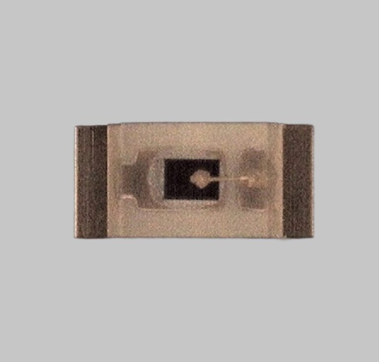
Does your application require tight binning? In this post, we will explore how specific wavelengths can optimize your product’s performance. We will explain how your choice of chip and other factors, including how you drive the component, will affect degradation and the lifetime of your product. What chip mounting options are best-suited for your application? This post will cover wire bonding techniques, die attach (eutectic or conductive paste), illumination patterns, and output. A complete listing of emitter chips ranging from deep UV to the visible range to near-infrared and short wave infrared (SWIR) also will be discussed in detail. Or you can visit our online Product Selector Guide now.
Part 2: Custom detection materials
The custom design of the detector chip is a capability unique to Marktech. In this post, we will cover the custom materials that we use in our silicon detectors, including PIN photodiodes, photodiode arrays, Avalanche photodiodes, and other detector products. We’ll review your options to customize either N-type, P-type, or epi-materials to optimize chip design, meeting or exceeding your specifications for characteristics like minimum reflection, low-dark current, minimum series resistance, low capacitance, fast response, and low crosstalk. Learn more about custom detection materials from Marktech >>
Part 3: Packaging
Once you have chosen the chip, the packaging criteria comes into play next. You need to define what important criteria are needed, for example, space constraints. Packaging options include SMD (surface mount devices), COB (chip on board), through-hole devices, and TO-cans, including multi-chips, which may contain both emitter and detector chips.
Depending on your choice of chip and package, the experts at Marktech will ascertain what conditions you may be dealing with, such as heat dissipation and electromagnetic interference. In this post, we also will explore lensing options to modify radiation patterns, such as wide or narrow viewing angles, or custom illumination patterns. Learn more about our custom packaging capabilities >>
Part 4: Custom Assemblies
Does your application require multiple chips, either for emission or detection or both? What is the best material for your assembly: FR-4 to ceramic, flex, or metal core? Depending on your application, our custom design engineers will help you determine how many chips are required based on output and drive conditions. At Marktech, we have completed assemblies ranging from two chips to 140, however, there are no restrictions on the number of chips we can mount. Learn more about custom assemblies >>
Part 5: Design, Testing, and Binning
Not only can Marktech test for all optical and electrical parameters on both emission and detector components, materials, and assemblies, we also offer unique testing capabilities on detectors including spectral response up to 3000nm, quantum efficiency up to 3000nm, shunt resistance, dark current, and capacitance. On the emission side, we can offer complete testing on UV down to 250nm and up to 2600nm on SWIR devices.
Part 5 in the series will cover all of our services in design, testing, binning, and quality control. We will share details about our 10-step design and test process, which ensures that we tailor services around your specific needs and make recommendations to ensure your device is performing as intended. Learn more about Marktech’s testing and engineering services >>
Part 6: Getting Started
Part 6 in the series will be a wrap-up summary of Parts 1 through 5 and will highlight the next steps to take if you are interested in pursuing a custom device, beginning with initial discussions with one of our application engineers. We will discuss the various steps to bring your idea from concept to prototype to finished component or assembly. Or if you are ready to get started now, contact us today!