UV detectors are offered in a variety of TO metal-can type packages from TO-18 to TO-39 with special UV glass lens to insure optimum lifetime and the least amount of material degradation
With the ability to detect light in the UV, visible, and infrared spectrums, photo detectors, photo transistors, and photodiodes are being used in increasingly more applications.
Marktech offers the broadest range of emitters commercially available ranging from 235nm to 4300nm across the UV, visible, NIR, SWIR, and MWIR spectral ranges.
Our advanced line of visible LED products is engineered to deliver high-quality, energy-efficient lighting solutions across various applications from 400nm to 700nm..
Our NIR LED wavelength range is typically from 700nm to 1000nm, extending into wavelengths invisible to the human eye but crucial for numerous technological and scientific applications.
Our standard product offering includes wavelengths from 1020nm to 4300nm and operating currents ranging from 20mA to 350mA for high-power applications.
Our Point Source LEDs are specifically engineered for optical encoders, edge sensors, and other critical applications that demand highly focused light with minimal dispersion.
Multi-LED chips in a single package, our multiple wavelength LEDs are engineered to address a myriad of applications across the UV, visible, NIR, SWIR, and MWIR spectral ranges
Crafted with the latest LED technology, these rings provide adjustable illumination to meet specific needs, ensuring optimal visibility and enhancing the quality of your projects.
As a proud CREE LED Solution Provider for over a decade, Marktech offers comprehensive engineering support, including design, binning, and material selection, alongside custom packaging options for specialized applications.
CREE LED through-hole emitters, designed for high-temperature and moisture environments with UV-resistant optical-grade epoxy, offer a range of colors for versatile applications in signage and lighting.
CREE High Brightness (HB) SMD LEDs are the brightest, most reliable architectural, video, signage, scoreboard, roadway, and specialty LEDs available today.
CREE LED’s P4 series represents a leap in LED design, combining efficiency with aesthetic versatility to meet the demands of modern lighting applications.
Marktech’s CREE LED XLamp® offerings on aluminum core starboards simplify LED integration for designers, providing a range of colors and angles on compact boards for easy testing and implementation in varied lighting applications.
Marktech Optoelectronics introduces its new product line of CREE LED die, including the EZ1350 Series Die, packaged in TO-cans (TO-18 and TO-39 outlines) designed for precision and reliability in demanding applications with protection against environmental factors like moisture and dust.
Marktech Optoelectronics combines over 40 years of expertise in optoelectronics with a focus on customized engineering solutions, addressing specific customer needs and applications.
Custom photodiode detectors are designed to meet unique customer requirements, offering specialized performance features and cost savings through optimizations such as integrated filters, photodiode arrays, and hybridization.
Through our vertically integrated manufacturing facilities in California and Japan, we offer custom LED solutions, including packaging and optoelectrical categorization, enhancing product design and market readiness.
Multiple LED dies combined in a single package are engineered to address various applications across the UV, visible, NIR, SWIR, and MWIR spectral ranges.
To succeed, you need the exact optoelectronic package custom-designed and manufactured for your application, including hermetic metal SMD, TO-can, plastic SMD, and molded through-hole packaging.
Made-to-order semiconductor chips (die) and wafers are designed and fabricated to fit your needs. Standard dies are available in specific wavelengths for high-volume production applications.
List of common concepts and definitions for Photodiodes.
Buy Now
New Transfer-Molded LED and Photodiode Packages Enhance Optical Performance and Reliability – Available in 2026 from Marktech Optoelectronics
Coming soon in 2026 - Advanced Transfer Molded Optoelectronic Packaging
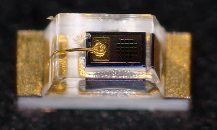
Prototype Transfer Molded Package (under development)
Latham, NY, and Kawasaki-Shi, Japan — January 6, 2026 Marktech Optoelectronics and their manufacturing partner Optrans Corporation are introducing new transfer-molded photodiode and LED packaging capabilities, currently under development and scheduled for first customer availability in Q2 2026. These next-generation photonics packages offer improved reliability, optical beam control, enhanced environmental robustness, and reduced stray-light interference while supporting both conventional LED emitters and advanced point-source RCLED and QWLED architectures.
Transfer molding forms a precision optical and mechanical structure directly over the die, encapsulating the LED or detector in a controlled molding process that produces exceptional part-to-part uniformity, tighter beam profiles, stronger wire-bond protection, and improved long-term reliability under temperature and humidity stress. This approach offers significant advantages over traditional packaging methods—such as glob-top epoxy, liquid potting, COB silicone domes, and discrete lens cap assemblies—making it especially well-suited for industrial, medical, instrumentation, aerospace, and automotive applications that require repeatable performance, a small footprint for dense packing, and robust handling.
“Transfer molding gives us exceptional control over optical geometry, reliability, and manufacturing scalability,” said Vince Forte, Chief Technical Officer at Optrans Corporation. “This is especially important for point-source LEDs where beam shape and emitter alignment directly impact system performance.”
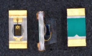
Example of new prototype transfer-molded package – (under development)
Key Advantages of Transfer-Molded Packaging
Improved Optical Performance Transfer-molded packages allow for integrated primary optics, enabling tightly controlled lens profiles for beam shaping, collimation, and fiber- or aperture-coupling. This is particularly valuable for RCLED and QWLED point-source emitters, where sub-millimeter optical alignment is required for measurement, medical, aiming, and sensing applications. The molding process also provides excellent control over emitter-to-lens alignment, ensuring that the optical axis is precisely maintained from unit to unit—critical for applications requiring tight beam symmetry or long-distance projection. Transfer-molded materials can be engineered for high UV, visible, or IR transmission, enabling improved radiant flux output and enhanced optical efficiency. In addition, the package structure reduces internal reflections and minimizes angular variation, resulting in more uniform and predictable emission profiles. Furthermore, phosphor additives can be incorporated directly into the molding compound to convert or broaden the LED’s native emission spectrum, enabling tailored spectral outputs—such as multi-band, white-light, or application-specific wavelengths—without the need for external filters or secondary optics.
Detection performance can also be optimized using a transfer-molded photodiode package. For instance, transfer-molded packages allow for integrated primary optics, enabling tightly controlled lens profiles for beam shaping, collimation, and coupling. In addition, the transfer-molded photodiode package minimizes stray light, reduces parasitic reflections, and maintains tighter alignment tolerances, resulting in higher signal-to-noise ratio and more accurate detection. It also provides consistent optical geometry and mechanical stability, ensuring repeatable responsivity and improved low-light performance. Transfer molded packaging can reduce parasitic capacitance because epoxy molding compounds typically have a lower dielectric constant (εr ≈ 3.5–4.5) compared to ceramic, glass-to-metal seals, or large metal package volumes. By reducing parasitic capacitance and enhancing thermal dissipation, transfer-molded photodiode packages further enable faster response times and greater precision in demanding sensing applications—all within a compact, reliable, production-scalable form factor. Furthermore, when the molding compound is formulated with optical filtering characteristics, it can function as an integrated bandpass or notch filter, selectively transmitting or blocking specific wavelengths to enhance detection accuracy in targeted spectral bands.
Better Reliability and Environmental Robustness Mechanical stability is also enhanced, as the molded compound encapsulates and protects the LED die, improving vibration resistance and long-term reliability in harsh environments. Wire bonds in conventional, non-encapsulated packages can fail by lift-off (wire debonding) or wire fracture due to mechanical stress from vibration, impacts, and thermal cycling. A monolithic molded package structure protects the die and wire bonds from shock, vibration, thermomechanical fatigue, and water ingress, resulting in enhanced durability and more consistent performance across temperature and mechanical extremes. This makes optoelectronic transfer molded packaging technology an ideal choice for automotive, industrial, aircraft, and defense-grade requirements.
Low Profile, Compact Footprint, and Dense Packing Transfer-molded SMD optoelectronic packages offer a significantly smaller footprint than many conventional SMD LED and photodiode package styles because the optical and mechanical structures—such as lenses, light shields, and housings—are formed directly in the molded body rather than added as separate plastic components. By eliminating bulky reflector cups, multi-part lens caps, and oversized lead frames, transfer-molded packages can achieve tight lateral dimensions and low profiles, often in standard JEDEC outlines optimized for automated pick-and-place.
This reduced footprint enables much denser component packing on printed circuit boards (PCBs), supporting higher channel counts in sensing arrays, more compact illumination modules, and miniaturized instrumentation. As electronics continue to shrink in size and increase in functional complexity, the compactness of transfer-molded SMD optoelectronics provides a critical advantage—allowing designers to integrate more optical functionality into smaller form factors without sacrificing performance or reliability.
Manufacturing Consistency and Cost Efficiency Compared to liquid or manually formed encapsulants, transfer molding provides repeatable geometry, minimal unit-to-unit variation, and scalability for high-volume production. Once tooling is in place, the process yields lower per-unit cost with tight control over height, planarity, lens radius, and package outline.
Availability Engineering prototypes are planned for release in early 2026, with full production availability beginning in Q2 2026. Transfer-molded photodetector, and LED packages will be available in select JEDEC and IPC SMD footprints. Custom sizes and optical geometries can be developed to OEM design specifications. Additional potential photonics packaging variations include options for integrated lenses, phosphor layers, filter windows, and light shielding. Initially, chip sizes up to 350 µm × 350 µm can be packaged. Our new transfer-molded packaging is suitable for emission and detection from 355 nm to 2300 nm.
Engineering samples and custom design engagements are welcome upon request. In the U.S. contact: Marktech Optoelectronics Email: [email protected]
In Japan and International Locations contact Optrans Corporation Email: [email protected]
About Marktech Optoelectronics Marktech Optoelectronics, headquartered in Latham, NY, specializes in the design, testing, and manufacturing of optoelectronic components, including LEDs, emitters, detectors, and custom assemblies. Marktech partners closely with engineering teams to provide performance-optimized photonic solutions tailored to specific application needs. Website: https://marktechopto.com
About Optrans Corporation Optrans Corporation, located in Kawasaki-Shi, Japan, is a high-precision optoelectronic device manufacturer with advanced semiconductor processing, assembly, and optical packaging capabilities. Optrans supports high-reliability and high-performance optoelectronic production for global customers across sensing, instrumentation, industrial, and medical markets. Website: https://optrans.co.jp
Visit Our Booth at Photonics West 2026 to Learn More About Our Photonics Packaging Capabilities
Plan now to visit our booth (#259) at SPIE Photonics West, 17 – 22 January 2026 in San Francisco, California to help us celebrate 40 years of photonics innovation. SPIE Photonics West is the optics and photonics industry’s flagship exhibition to meet the sector’s biggest names and learn about the latest innovations.
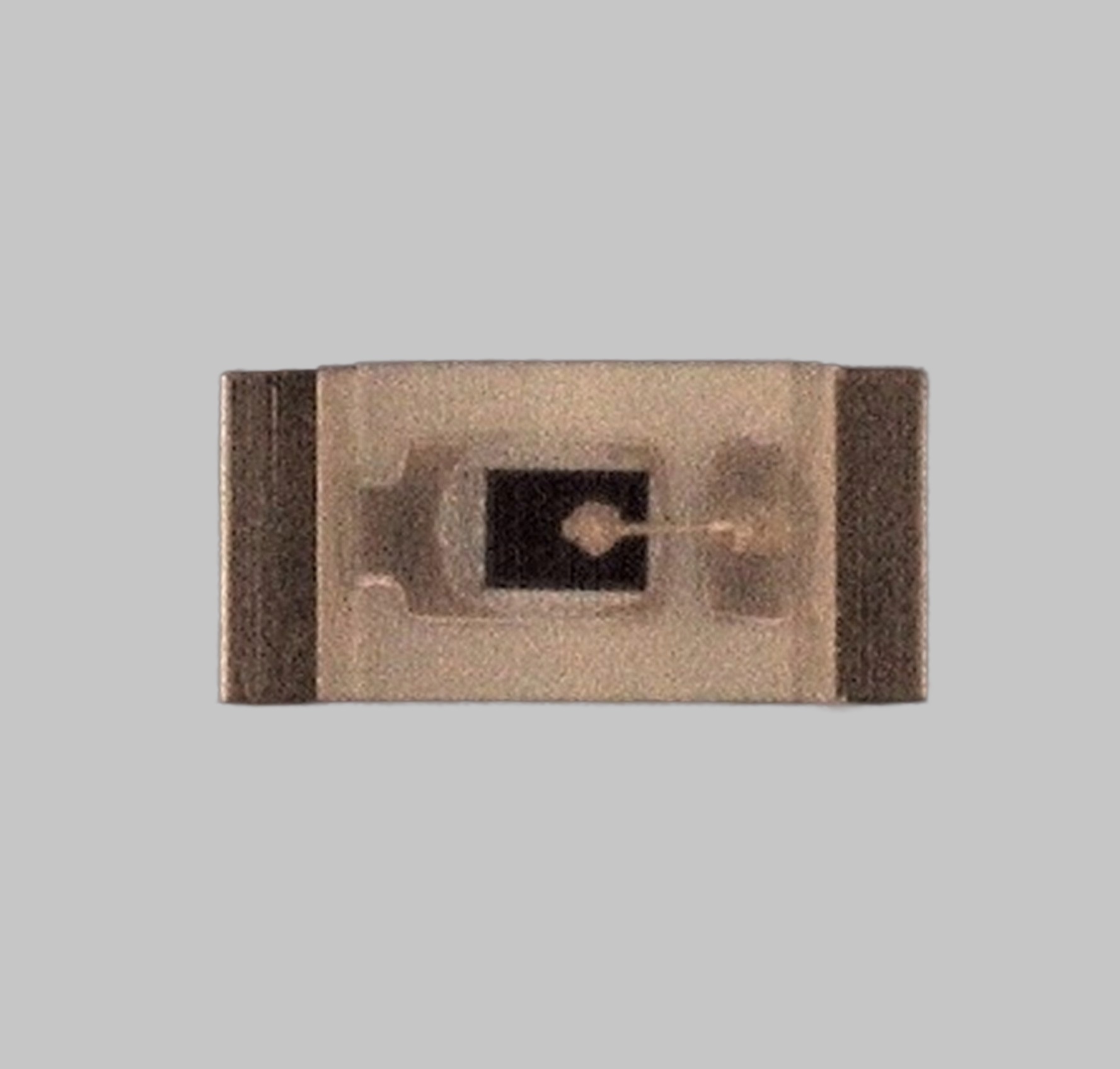
New Transfer Molded Packaging Enables Breakthrough Performance in Precision Optical Sensing Example of our transfer molded package structures LATHAM, NY – June 2, 2026 –
Marktech Optoelectronics, a leader in innovative light-emission and detection solutions, today announced the launch of several new 280nm UVC LEDs in single-, two-chip, and four-chip
Industry-Leading UV LEDs Enabling New Designs for Curing, Sensing, and UVGI Disinfection Systems Latham, NY — February 25, 2025 – Marktech Optoelectronics (“Marktech”), a leader
Technical BriefBy Gary Kardys, CMO Using UVC as a “miracle sterilizer” without accounting for efficacy, safety standards, exposure limits, regulatory constraints, and proper engineering controls
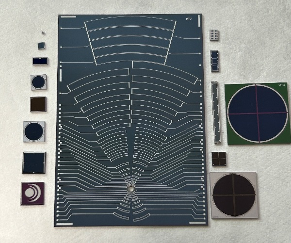
Industry-Leading Active Areas Enable Breakthrough Performance in Precision Optical Sensing LATHAM, NY – January 6, 2026 – Marktech Optoelectronics, a pioneer in advanced photodetector and
Manage Consent
To provide the best experiences, we use technologies like cookies to store and/or access device information. Consenting to these technologies will allow us to process data such as browsing behavior or unique IDs on this site. Not consenting or withdrawing consent, may adversely affect certain features and functions.
Functional
Always active
The technical storage or access is strictly necessary for the legitimate purpose of enabling the use of a specific service explicitly requested by the subscriber or user, or for the sole purpose of carrying out the transmission of a communication over an electronic communications network.
Preferences
The technical storage or access is necessary for the legitimate purpose of storing preferences that are not requested by the subscriber or user.
Statistics
The technical storage or access that is used exclusively for statistical purposes.The technical storage or access that is used exclusively for anonymous statistical purposes. Without a subpoena, voluntary compliance on the part of your Internet Service Provider, or additional records from a third party, information stored or retrieved for this purpose alone cannot usually be used to identify you.
Marketing
The technical storage or access is required to create user profiles to send advertising, or to track the user on a website or across several websites for similar marketing purposes.