Marktech Expands their Multi-chip Product Line with Multi-Wavelength SWIR LEDs and a 2.6µm InGaAs Detector in One Package

Marktech’s Next Gen Hermetic SMD ATLAS Packaged InGaAs Detectors

Marktech MTMD34679PD6T38 – SWIR multi-chip emitter-detector with multiple wavelength LEDs

April 23, 2024 – Latham, NY, USA –  Marktech Optoelectronics, Inc. (www.marktechopto.com)(Marktech), a privately-held leading designer and manufacturer of standard and custom optoelectronics, including UV, visible, near-infrared (NIR), and short-wavelength infrared (SWIR) emitters, detectors, InP epi wafers, and other compound semiconductors, today reveals their new multi-chip packages combining InGaAs photodiodes and multiple SWIR LEDs in the same package. These products join a growing line of multi-chip products consisting of multi-wavelength LEDs (UV through MWIR) with or without InGaAs, silicon, or InGaAs+silicon detectors.

Our range of multi-chip products includes:

  • Multiple LEDs in a single package (235nm to 4300nm wavelength combinations)
  • Multiple detectors in a single package (multiple silicon, InGaAs, and SiC photodiodes)
  • Multiple LEDs + single or various detectors in a single package
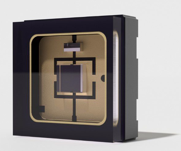
  • Packaging options include SMD, TO-can, and our award-winning ATLAS hermetic SMD

ATLAS hermetic SMD packages are ideal for LED, detector, & multichip applications.


Co-Packaged InGaAs Photodiodes with Multiple LED Emitters

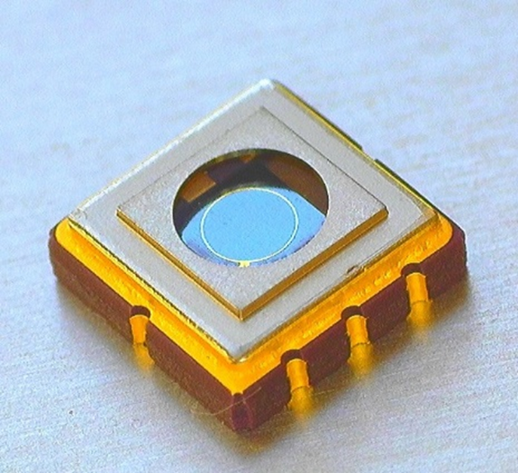
Our newest multi-SWIR LED emitters + detector components include part numbers MTMD1479PD6T38 and MTMD34679PD6T38. MTMD1479PD6T38 includes 1460nm, 1720nm, and 1900nm SWIR LED chips combined with a 2.6µm InGaAs detector providing 800nm to 2600nm responsivity. MTMD34679PD6T38 has the same 2.6µm InGaAs detector co-packaged with 1300nm, 1460nm, 1650nm, 1720nm, and 1900nm SWIR LEDs. To the best of our knowledge, our 2.6µm InGaAs detector has the highest responsivity on the market based on our internal tests and customer evaluations comparing our InGaAs detectors with our competitor’s products.

Marktech’s UV, visible, NIR, and SWIR emitters combined with our IR detectors (InGaAs photodiodes) are the perfect solution for many analytical, medical, aerospace, and industrial sensing applications. An additional silicon detector can be added to the package when UV LED light needs to be monitored or detected. The co-packaged emitters are individually addressable. Multiple chip products are available in TO can and SMD packages.

Multiple Wavelength Multi-chip Products

For applications such as transmission spectroscopy requiring a multiple-wavelength source separate from the detector, Marktech also produces multi-wavelength -devices consisting of multiple LED chips in a single package.

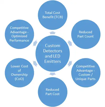
Our newer LED light sources, Multiple wavelength LED emitters, have several advantages over singularly packaged LEDs and older, conventional light sources. Co-packaging multiple LED emitters can:

  • Ability to rapidly vary light power output and wavelength
  • Reduce Circuitry & Simpler Design
  • Reduce Part Count
  • More compact design – ideal for wearable applications
  • High-speed wavelength selection
  • No or minimal heat dissipation – reduce heat compared to halogen, xenon, mercury vapor, or thermal IR emitters
  • Reduce power compared to halogen, xenon, mercury vapor, or thermal IR emitters
  • Increase life compared to halogen, xenon, mercury vapor, or thermal IR emitters
  • Fast response (on/off or pulsing) – no warm-up delay of halogen, xenon, mercury vapor, or thermal IR emitters
  • Elimination of moving parts – e.g., motorized slit in dispersive spectrometers
  • High emission stability – no or minimal wavelength drift over the lifetime

Our multiple LED and multi-detector products are available in several variations:

  1. Multiple emitters combined with InGaAs photodiodes for Vis-NIR-SWIR detection
  2. Multiple UVC LEDs (235nm, 255nm) with SiC photodiodes for deep UVC emission and detection
  3. Multiple emitters joined with silicon photodiodes for UVB-Vis-NIR emission and detection
  4. Multiple emitters sharing the same package with both InGaAs and silicon photodiodes for UVB-Vis-NIR-SWIR detection
  5. Multiple InGaAs, silicon, and InGaAs-silicon detector combinations with different emission filters on each photodiode
  6. Multiple InGaAs, silicon, and InGaAs-silicon detector combinations with integral transimpedance amplifiers (TIAs)
  7. Multiple InGaAs, silicon, and InGaAs-silicon detector combinations with thermionic coolers
  8. Multiple LED emitters of multiple wavelengths
  9. Multiple LED emitters of the same wavelength for increased power

Multiple emitters in one package ( up to 7 in our standard thru-hole or SMT package) along with detectors in a separate package (4, 5, & 6) can be helpful in colorimeter and color photometer applications using cuvettes where the excitation light is transmitted through the sample – or, where the excitation wavelength(s) needs to separate from the photodiode detector(s).

The specific combinations of emitters and detectors can be tailored or “mixed and matched” to your application’s specific light source and detection requirements.

In applications requiring higher power, multiple LED die of the same wavelength are placed in the same package. For example, Marktech’s MTMD4270T38 product contains two 428nm LEDs and two 700nm LEDs. Our MTMS1300N24 SWIR LED emitter contains three 1300nm chips in a narrow domed lens TO-can package. Our  MTMD7885T38 multiple wavelength emitter has three 770nm die in a PLCC package. Our MTMS7700T38 (770nm), MTMS8800T38 (880nm), and MTMS9400T38 (950nm) products utilize six LED emitter chips in the TO-can package.

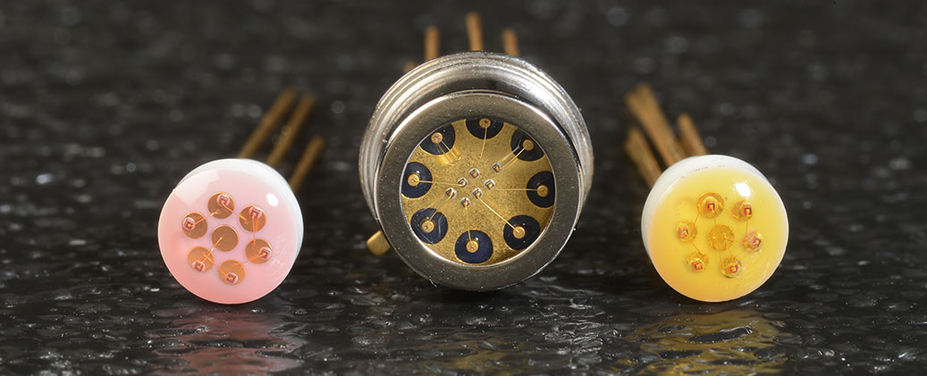
Examples of Marktech’s multiple wavelength, multi-chip LED products

InGaAs detectors and InGaAs photodiodes with multiple LEDs are beneficial in a variety of applications, such as:

  • Biomedical instrumentation
  • Black ice detection
  • Broadband, hyperspectral, and multispectral light sources
  • Colorimetry
  • Contamination or foreign material detection
  • Counterfeit currency detection
  • Curing / Crosslinking
  • Endoscopic lighting and tissue oximetry
  • Fluorometry
  • Fluorescence microscopy
  • Functional near-infrared spectroscopy (fNIRS)
  • FURA / calcium imaging
  • Glucose monitoring
  • Industrial machine vision
  • Iris matching or recognition for biometrics
  • NIR spectrometry
  • Optical communications
  • Optogenetics
  • Oximetry / Co-oximetry
  • Photodynamic therapy
  • Photometry
  • Solar simulation
  • Sorting equipment
  • Spectroscopy
  • SWIR Detection
  • SWIR Imaging

In some applications, the integral detector acts as a monitor to indicate the LEDs are emitting light. In other cases, the InGaAs can detect reflected or fluorescence emission from a sample illuminated by the LEDs. For example, oximeters, NDIR, and fNIR devices can emit and detect the reflected or partially transmitted light to determine oxygen levels in the tissue. For applications that require light transmitted through a sample and then detected, Marktech can package the LEDs and InGaAs detectors separately.

In dispersive spectroscopic analysis, a monochromator generates a wide range of wavelengths. Monochromators employ a prism or diffraction grating combined with a motorized slit to select a specific excitation wavelength. Typically, we look at the peaks of an unknown chemical or material analyte and compare them to libraries of identified reference spectra.

In specific applications with unknown amounts of known analytes in a closed system, only a few specific wavelengths are required to distinguish between and quantify particular chemical constituents. Examples of applications where a selection of specific wavelengths is helpful in chemical analyte quantification include:

  • Spectroscopically analyzing the amount of reactant in a chemical production process
  • Colorimetric analysis of process, drinking, or wastewater contaminants
  • Oximetry, optical glucose monitoring, ischemia detection, and other medical diagnostics
  • Fluorometry for fluorescence identification of minerals or biological materials
  • Fluorescence microscopy for life science imaging (cells, proteins, biological materials)
  • Non-dispersive infrared (NDIR) spectroscopy-based gas analyzers or gas sensors

In one of these “closed systems” with multiple analytes, sometimes the more efficient option is not to choose wavelengths corresponding to the peaks of the analytes but rather a few wavelengths producing the most significant differences between the analyte’s absorption, reflectance, transmission, or fluorescence. With this methodology, fewer LED emitters can often provide better analytical results. In addition, the ratio transmission results from two or more wavelengths can account for slight interference in turbid or dirty samples.

Drawing of MTMD34679PD6T38 2.6µm InGaAs detector multiple wavelength LEDs


Multiple LEDs in Spectrometry, Fluorimetry & Fluorescent Microscopy

Eliminating the monochromator combined with LED emitters’ higher natural monochromatic nature can produce a higher power excitation light source than a dispersion spectrometer with broadband xenon, halogen, and mercury sources. In dispersion spectrometers, conventional light sources are broken into 128 or 256 wavelengths, with each wavelength having only a fraction of the energy of the source. Higher-power LEDs at specific peak wavelengths can improve the signal-to-noise ratio.

When comparing or discerning two analytes, specific wavelengths provide no additional information when the absorption levels of the two species are equivalent. Therefore, eliminating these wavelengths and using a few critical discerning wavelengths can speed up the overall detection process.

In addition, since a handful of the target excitation wavelengths are picked, each wavelength source can be optimized for high power output and increased wavelength monochromaticity. For instance, additional LEDs with the same wavelength can be packaged in the same TO can, PLCC, or SMD package to provide higher power for a particular wavelength. In addition, Marktech can sort or bin LED emitters to produce tuned LEDs with minimal peak wavelength variation of ±1nm. In higher-volume applications, wavelength variation and power output can be adjusted at the wafer level or in the light-emitting diode fabrication process. Likewise, InGaAs and silicon detectors can be customized during semiconductor fabrication to specific sensitivity ranges – when production volumes warrant the development.

Fluorometers (fluorescence spectrometers) and microscopes utilize a specific excitation wavelength capable of exciting a fluorescent dye or fluorophore in a sample, emitting at a peak emission wavelength. Cells, tissues, and other biological samples are often examined with fluorescence. LEDs eliminate several problems in fluorescence studies compared to older light sources, such as overexposure to light, thermal damage and phototoxicity of the biological sample, and photobleaching of fluorescent dyes or proteins. The peak wavelength of the LEDs can be selected to match the excitation wavelengths of the fluorophores closely. Combined with the higher intensity or power output at the peak wavelength, the result is improved signal-to-noise in fluorometry and fluorescence microscopy applications. Our multi-wavelength LED packages enable the selection of a different excitation wavelength for different fluorophores, fluorescent dyes, or color-indicating reagents. For instance, our MTMD2336T38 multi-wavelength light source can selectively emit 275nm, 310nm, 360nm, and 380nm wavelengths, and our MTMD3334T38 multi-wavelength light source can selectively emit 310nm, 360nm, 380nm, and 430nm wavelengths.

NIR and incredibly SWIR wavelength light can penetrate deeper into human tissue than visible light due to the reduced photon scattering at these wavelengths. SWIR’s high penetration depth enables imaging and spectral information collection deep into tissues. Some of these NIR/SWIR infrared imaging systems have mapped blood flow in live animals and imaged tissue 5mm into mouse brains. In addition, infrared spectroscopy can provide information on deep tissue chemical composition, such as oxygenation and deoxygenation. In the article, “Shortwave infrared fluorescence imaging with the clinically approved near-infrared dye indocyanine green,” the researchers stated that “imaging in the shortwave IR (SWIR; 1,000–2,000 nm) promises higher contrast, sensitivity, and penetration depths compared with conventional visible and near-IR (NIR) fluorescence imaging.” The researchers used NIR and SWIR light sources with an InGaAs detector. Marktech has many singular and multi-wavelength LED emitters in the NIR and SWIR wavelength ranges. For example, the Marktech MTMD142345PDT38 multiple SWIR wavelength emitter-detector contains 1040nm, 1200nm, 1300nm, 1460nm, and 1550nm peak wavelength LEDs combined with our InGaAs photodiode for SWIR detection in the 600nm – 1750nm range. These SWIR emitter-detectors can be helpful in tissue oxygenation and utilization studies using NIRS methods.

In summary, spectrometry, fluorescence microscopy, and other optical analytical methods performed with a specific set of multiple LED light sources and the appropriate photodiode detector can have improved signal-to-noise ratio and detection speed.

Consult with Us Today About Your Design Project

Marktech Optoelectronics has vertically integrated capabilities for custom design and fabrication of InGaAs photodiode detector devices on wafers and fabless capabilities in silicon and silicon carbide. After fabrication, we dice and package these photodiode chips with the required LED emitters, amplifiers, filters, and other hybridization components for specific applications. This vertical integration allows Marktech to precisely control the performance and quality of the photodetectors and assemblies designed and manufactured for our customers.

Using Marktech Optoelectronics advanced silicon and InGaAs photodetectors in new products under development will likely lead to breakthrough designs in many analytical instruments, medical diagnostics, and industrial sensing applications.

If you have specific technical or application questions regarding your optoelectronics design project or are just interested in learning more about Marktech’s silicon, SiC, and InGaAs photodiodes with multiple wavelength LED emitters, then please reach out to us through the following:

Maximize Your Total Cost Benefit with Tailored Photodiodes and LEDs for OEM Designs

Maximize Your Total Cost Benefit with Tailored Photodiodes and LEDs for OEM Designs

Photodiodes and LEDs are widely used in a range of applications, including optical sensors, communication systems, medical diagnostic devices, analytical instruments, and application specific lighting. They are often used together to maximize the total cost benefit, with photodiodes serving as detectors and LEDs as emitters. By tailoring these components to OEM design needs, engineers can optimize performance while minimizing costs.

Photodiodes are semiconductor devices that convert light into an electrical current. They are commonly used in applications such as light detection and communication systems, where they can be used to detect changes in light intensity or to transmit data via optical signals. Photodiodes can be designed with different materials and structures, such as silicon, SiC, or InGaAs, to optimize their sensitivity and response time for specific applications.

LEDs, on the other hand, are semiconductor devices that emit light when a voltage is applied to them. They are commonly used as light sources in a range of applications, including displays, lighting, and communication systems. LEDs can also be designed with different materials and structures, such as GaN or InGaN, to optimize their emission wavelength and brightness for specific applications.

By combining photodiodes and LEDs together in the same package, engineers can create efficient and cost-effective systems. For example, in a communication system, an LED can be used to transmit data via optical signals, while a photodiode can be used to receive the signals and convert them back into electrical signals. By selecting the appropriate photodiode and LED components for the system, engineers can optimize the performance and cost of the system.

What is total cost benefit?

“Total cost benefit” refers to a comprehensive evaluation of both the financial and non-financial gains that can be derived from an investment, action, or decision, in relation to the total costs involved, including financial expenditures and potential risks. This approach does not just look at the monetary aspect but also considers other benefits such as improved safety, convenience, or time savings, while accounting for all associated costs including potential downstream or auxiliary costs.
To obtain a true sense of the total cost benefit, one needs to examine all potential gains and savings, direct and indirect, tangible and intangible, that may result from the decision, and then compare it against a fully loaded cost profile that encompasses every possible cost, direct and indirect, associated with that decision.
A total cost benefit analysis aims to provide a more rounded view of the value proposition of a decision by exploring it from multiple dimensions, and it is a critical tool in both business and policy making, aiding stakeholders in making informed decisions grounded on a holistic understanding of the potential outcomes. It offers a macro perspective, enabling a thorough evaluation and thereby facilitating choices that are aligned with long-term objectives and holistic wellbeing.

Maximizing Total Cost Benefit with Customization

To maximize the total cost benefit of photodiodes and LEDs, engineers should carefully consider the specific needs of their OEM designs. This includes selecting components that are optimized for the specific application, as well as components that are cost-effective and reliable. It also involves selecting components that are easy to integrate into the overall system design, with minimal additional components required.

For example, in a sensing system, the photodiode and LED components should be selected based on the desired sensitivity and wavelength range of the system. The components should also be selected based on their reliability and cost, with consideration given to the overall cost of the system. Additionally, the components should be designed with ease of integration in mind, to reduce the overall system complexity and cost. Standard or lower cost optoelectronic components often do not minimize the total system cost of a design or the “total cost of ownership”. For example, a design engineer may have planned on buying two separate photodiodes to meet the detection wavelength range requirements of the project. Marktech’s custom solution combined two photodiodes in the same package resulting in a lower total cost and less complicated design compared to purchasing two separate detectors.

In some cases, a detector has more gain than is required for a project. For these optoelectrical design projects, Marktech has custom developed lower active area detectors, which are less costly than a standard photodiodes with larger active areas.

Bacteria or microbes can have sensitivity to destruction at certain wavelengths. For instance, cryptosporidium is sensitive to or most effectively killed by 265nm light. In some sanitization cryptosporidium applications, mercury vapor lamps with a wide spectrum are used. Power is wasted because some of the wavelengths emitted are ineffective at destroying the bacteria Marktech can provide 265nm LEDs specifically targeting cryptosporidium eliminating providing a design with more energy efficiency and longer battery life. Likewise, Marktech can provide 235nm and 255nm deep UVC wavelengths for the detection of creatine, uric acid, proteins, nitrates in water or blood samples.

In addition, off-the-shelf parts frequently cannot provide the optimized performance of a bespoke detector or LED developed specifically for a new electro-optical product design. Even if the overall cost of the system is slightly higher using a custom part than a standard component, the performance per cost is higher or the total cost benefit is lower.

An intangible benefit is the competitive advantage provide provided by unique, custom LEDs or photodiodes. Bespoke optoelectronic parts can provide unique optoelectrical characteristic unlike any catalog type components. A design with a standard component can be more easily reversed engineered and then duplicated. Custom LEDs or custom detectors cannot be duplicated as easily or at all in some cases.

Tailoring LEDs and photodiodes to the specific design requirement can eliminate the need for additional component such as optical filters, amplifiers, lenses, etc. – resulting in lower system cost, higher product performance, or higher total cost benefit.

Photodiode Customization

  1. Material Selection: Photodiodes can be fabricated from different semiconductor materials, such as silicon, germanium, or InGaAs, depending on the wavelength range and sensitivity requirements of the OEM design. Each material types has characteristic ranges of wavelength sensitivity.
  2. Multi-detector Design: When a wide spectrum of wavelengths need to be detected, multiple wavelengths can be combined. Marktech can combine silicon and InGaAs photodiodes to provide a single detector package capable of detecting from
  3. Structure Design: The structure of the photodiode can be tailored for specific applications, such as PN photodiodes, PIN photodiodes, and avalanche photodiodes (APDs) to optimize for sensitivity, dark current, and response time.
  4. Optoelectronic Packaging: Photodiodes can be packaged in different formats, such as surface-mount packages, chip-on-board (COB), or ceramic packages, to meet the size and integration requirements of the OEM design.
  5. Active Area Size: The size of the active area of the photodiode can be customized to match the size of the light source or target in the OEM design, to optimize the detection efficiency. Photodiode for monitoring non-visible UV or IR light sources, often a very small area is sufficient. In applications where the transmitted or reflected light is very weak, a larger active area or multi-element photodiode can be developed to optimize photodetector response.
  6. Responsivity and Dark Current: The responsivity and dark current of the photodiode can be optimized by adjusting the doping concentration, bias voltage, or temperature, to meet the sensitivity and noise requirements of the OEM design.
  7. Optical Filters: Optical filters, such as bandpass filters or notch filters, can be integrated with the photodiode to improve the selectivity and reduce noise.
  8. Reverse Bias Voltage: The reverse bias voltage of the photodiode can be adjusted to control the sensitivity and saturation level, depending on the light intensity range of the OEM design.

By tailoring or customizing photodiodes to OEM specifications, engineers can optimize the performance and cost of their systems. The specific tailoring options chosen will depend on the specific application and requirements of the OEM design.

Table summarizing the customization types for photodiodes and their respective ranges/examples:

Customization TypeRange/Example
Material SelectionSilicon, InGaAs, Other
Multiple DetectorsSi+InGaAs PDs, multiple SiPDs, multiple InGaAs PDs
Structure DesignPN, PIN, Array photodiode structures
PackagingSurface-mount package, Chip-on-board (COB), Ceramic package, ATLAS Hermetic SMD package
Active Area Size0.1 mm² to 100 mm²
Responsivity and Dark CurrentResponsivity: 0.1 A/W to 1 A/W, Dark Current: pA to µA
Optical FiltersBandpass filter, Notch filter
Reverse Bias Voltage1 V to 100 V


Note that the ranges/examples provided are not exhaustive and may vary depending on the manufacturer and specific application requirements.

LED Emitters Customization

  1. Light emitting diodes (LEDs), also known as emitters, can be tailored or customized to meet specific OEM specifications in various ways. Here are some examples::

    1. Material Selection: LEDs can be fabricated from different semiconductor materials, such as GaN, InGaN, or AlInGaP, depending on the desired emission wavelength and brightness of the OEM design.
    2. Sorting/Binning: LEDs can be sorted or binned to ensure consistent performance within a specific range of parameters, such as emission wavelength or brightness.
    3. Structure Design: The structure of the LED can be tailored for specific applications, such as high-brightness LEDs or surface-emitting LEDs, to optimize the brightness and efficiency.
    4. Packaging: LEDs can be packaged in different formats, such as TO-can, plastic through hole, PLCC SMD, COB, or multichip-multiwavelength, depending on the size and integration requirements of the OEM design.
    5. Lens Types: The LED can be equipped with different lens types, such as flat, dome, or ball lenses, to optimize the light output and directionality for the OEM design.
    6. Substrate Material: The substrate material of the LED can be customized to improve thermal management, such as using silicon carbide (SiC) or diamond substrates for high-power LEDs.
    7. Current Density: The current density of the LED can be adjusted by changing the size and number of the semiconductor layers, to optimize the brightness and efficiency for the OEM design.
    8. Thermal Resistance: The thermal resistance of the LED can be optimized by selecting appropriate packaging and substrate materials, to ensure stable and efficient operation under different environmental conditions.
    9. ESD Protection: The LED can be equipped with electrostatic discharge (ESD) protection features to improve its reliability and durability in high-voltage or high-static environments.
    10. Customized Pin Configuration: The pin configuration of the LED can be customized to suit the OEM design’s specific requirements.
    11. ATLAS Hermetic SMD Packaging: ATLAS Hermetic SMD packaging can be used to create more rugged and durable LED packages that can withstand harsh environments.

    Table summarizing LED customization types and their respective ranges/examples:

    Customization Type

    Range/Example

    Material Selection

    GaN, InGaN, AlInGaP

    Sorting/Binning

    Emission wavelength sorting tolerance: +/- 1 nm

    Structure Design

    High-brightness LED, Surface-emitting LED

    Packaging

    TO-can, Plastic through hole, PLCC SMD, COB, Multichip-multiwavelength, ATLAS Hermetic SMD package

    Lens Types

    Flat, Dome, Ball lenses

    Substrate Material

    Aluminum oxide, ALON, SiC, etc.

    Current Density

    1 A/cm² to 100 A/cm²

    Thermal Resistance

    0.1 K/W to 10 K/W

    ESD Protection

    > 4 kV HBM (Human Body Model)

    Customized Pin Configuration

    2-pin, 3-pin, 4-pin, etc.

    ATLAS Hermetic SMD Packaging

    Rugged and durable packaging that can withstand harsh environments

    Note that the ranges/examples provided are not exhaustive and may vary depending on the manufacturer and specific application requirements.

Conclusion

photodiodes and LEDs are powerful tools for optimizing the cost and performance of OEM designs. By selecting the appropriate components and tailoring them to the specific needs of the application, engineers can create efficient and cost-effective systems. With careful consideration of the performance and cost trade-offs, photodiodes and LEDs can be used to create systems that maximize the total cost benefit for OEM designs with the additional benefit of providing unique features, which are difficult for competitors to duplicate.

2023 Achievements – Meet Us At Photonics West 2024 to Learn More

Happy New Year’s Wishes from the Marktech Optoelectronics team!

If you are attending SPIE Photonics West in January, then stop by our booth (#237) from January 30 thru February 1 at the Moscone Center in San Francisco, California. SPIE Photonics West is the world-renowned event for the photonics, optics, emitters, and detectors field.

We will showcase our latest product innovations and out technical experts will be on hand to answer any questions related to your detection or emission design projects.

Here are a few of our notable achievements and innovative new product introduced in 2023:
Advanced 235nm and 255nm UVC LEDs from Silanna: The Future of Germicidal UV Solutions

Marktech Optoelectronics ATLAS Hermetic SMD Packaged InGaAs Photodiodes Win 2023 Best of Sensors Awards in the Aerospace and Space Category

Marktech Optoelectronics Announces the Launch of Innovative Quadrant Silicon Photodiode – MT03-072

Marktech Optoelectronics Offers Latest CREE LED High Brightness Visible LED Innova (TO Can and ALTAS Hermetic SMD Packaging Options Available Where Applicable)

Marktech Optoelectronics Releases New Green and Red Dot LEDs

Marktech Introduces Multi-chip Multi-wavelength SWIR LEDs with Integral Monit InGaAs Photodiodes for Chemical Analysis and Medical Diagnostics

Marktech Optoelectronics Expanding the Industry’s Broadest Line of Point Source LEDs with New Hermetic SMD Packaged Visible and Infrared Emitters

Marktech Unveils New Four Chip Photodetector with InGaAs+Silicon Photodiodes in ATLAS Hermetic SMD Packaging

Marktech Expands Line of Multi-chip Products with New Additions of Multi-chip Multiple Wavelength (UV-Vis-NIR-SWIR) LEDs and Multi-chip SWIR LEDs with Monitoring Photodiodes

Marktech Expands Internationally Signing Agreements with Trading and Sales Engineering Representative Groups in Japan, Israel, Canada, and the European Union

Marktech Reveals a New 2.6µm InGaAs Assembled Quadrant Photodiode
Marktech Optoelectronics Releases Enhanced Sharpness 25 & 50 Micron Red Dot LEDs – Standard & Customizable Designs

Marktech Optoelectronics will be showcasing both their well-established and newly released products and capabilities, such as:

Optical detectors (UV, Visible, & Infrared Detectors)

Short Wave Infrared (SWIR) LEDs Emitters

  • SWIR LEDs – 1020nm to 1720nm
  • Extended SWIR LEDs – 1900nm to 2600nm – Coming in 2024

Multi-wavelength and Multiple Chip Emitters and Detectors

Mid-Wave Infrared (MWIR) LEDs/emitters – Coming in 2024

Point Source LEDs (PSLs)

Near Infrared (NIR) Emitters

Visible LED Emitters – 400nm to 650nm

Red dot LEDs, reticle LEDs, and alphanumeric LED micro-displays

CREE-LED high-brightness LEDs in a wide range of forms:

  • Through-hole, metal can, starboard, linear boards, and custom packages & assemblies

SMD UV LEDs and Through-hole UV LEDs

SMD UV LEDs and Through-hole UV LEDs

Advanced optoelectronic packaging capabilities

Custom OEM Solutions – Optoelectronics Design, Engineering, Device Fabrication & Packaging

Compound Semiconductor Materials

  • Indium Phosphide (InP) Epitaxial Wafers for PIN Photodiodes
  • APD Structured InP Epi-wafers

Optoelectronic Chip Design & Fabrication (Photodiodes, Phototransistors, Custom Devices)

Wide Spectral Range Optoelectronic Testing Services – Both Detectors & LED Emitters

New 2.6µm InGaAs PIN Photodiode Quadrant Introduced in 2023.

Marktech Optoelectronics, Inc. (www.marktechopto.com)(Marktech), is a privately-held and veteran-owned leading designer and manufacturer of standard and custom optoelectronics, including UV, visible, near-infrared (NIR), and short-wavelength infrared (SWIR) emitters, detectors, InP epi wafers, and other compound semiconductors.

Please drop by our booth or contact us any time if you:

  • Have any technical or application questions or need assistance regarding any of your optoelectronic design projects
  • Require validation of the optical characteristics (wavelength, power output, sensitivity) of your current optoelectronics components (emitters or detectors)
  • Are you interested in learning more about Marktech’s cutting-edge InGaAs SWIR detectors, SWIR LED emitters, ATLAS hermetic SMD packaging, silicon photodetectors, chip-scale packaging (CSP), or multi-wavelength & multi-chip (MWMC) packaging
  • Want to schedule a time to consult with our engineering experts at the Photonic West:
    Contact Tom Behringer at [email protected]

If you have an urgent project or component questions: Contact Us.

Advanced 235nm and 255nm UVC LEDs: The Future of Germicidal UV Solutions

Marktech Optoelectronics Launches Advanced 235nm and 255nm UVC LEDs:
The Future of Germicidal UV Solutions

[Latham, NY, November 14,2023] – Marktech Optoelectronics, a leader in innovative light emission and detection solutions, proudly announces the release of cutting-edge 235nm and 255nm UVC LEDs from Silanna housed in flat and dome lens SMD and TO-cans packages (e.g., MTE2350F-UV and MTE2350D-UV). This release heralds a new era in germicidal UV applications, offering superior benefits over traditional UV lamps. The Silanna Safe™ 235nm emitting chips inside these UVC LEDs provide outstanding power efficiency without the skin cancer risks associated with higher wavelength UVC LEDs.

Silanna UVC LED in flat lens SMD package.

Designed for diverse applications, these UVC LEDs are set to revolutionize germicidal UV solutions and chemical sensing. Marktech can also provide the new 235nm and 255nm LEDs in custom packaging. In 2024, we will be releasing these groundbreaking UVC LED chips in a variety of packages including our award-winning hermetic metal-ceramic ATLAS package.

Applications include

A standout feature of Marktech’s UVC LEDs is their safety profile. Unlike UVB and UVA LEDs, unintentional overexposure to Marktech 235nm UVC results in only short-term redness and eye irritation, eliminating the risk of skin cancer and cataracts.

Key Advantages of Marktech's UVC LEDs

“Marktech’s commitment to advancing UV lighting technology is evident in these 235nm and 255nm UVC LEDs from Silianna. We’re not just offering a product; we’re offering a safer, more efficient, and environmentally friendly solution for many applications,” stated Vince Forte, Chief Technology Officer (CTO) at Marktech Optoelectronics.

Marktech encourages design engineers to develop products for water purification, air disinfection, gas sensing, and chemical analysis to explore the unmatched benefits of these revolutionary UVC LEDs.

For media inquiries, please contact:

Gary J. Kardys, Business Development Manager, [email protected], 518-956-2980 ext 237

Key Advantages of Marktech's UVC LEDs

Established in 1985, Marktech Optoelectronics has been at the forefront of light emission and detection solutions across a wide spectral range from UVC to SWIR. With a focus on quality, safety, and environmental sustainability, Marktech is constantly innovating and adapting to serve the dynamic needs of optical and electronic design engineers in the OEM space.

To learn more, please visit:  https://marktechopto.com/  

Marktech Introduces New Generation of SWIR Emitters

With ranges of 1040nm to 1650 nm, new series offers up to 2X increased power output compared to previous models

LATHAM, NY—Feb. 9, 2021—Marktech Optoelectronics, one of the world’s leading optoelectronics engineering, design, manufacturing and test facilities, today announced the introduction of its new series of short wavelength infrared (SWIR) Emitters. This next generation of SWIR Emitters offers ranges of 1040nm to 1650 nm, with increased power output of up to 2X with better reliability and lifetime than the company’s previous SWIR devices. SWIR is a relative new product technology. Due to its higher wavelengths, it allows the designer to detect materials ranging from water to glucose and agricultural products, among many examples.

“This is a significant milestone in the evolution of SWIR Emitter technology,” said a spokesperson for Marktech. “Each increase in range, coupled with advances in power output, leads to new and innovative use cases for the devices.”

The unique light produced by SWIR imaging can be put to work in electronic board inspection, surveillance, anti-counterfeiting and more. Among the target industries for SWIR devices are medical, industrial, agriculture, communications, security, and wearables. Marktech offers its series of SWIR emitters and compatible detectors through Digi-Key.

Marktech is one of a few limited manufacturers SWIR Emitters in these ranges. The company’s standard product offering includes both through-hole and surface mount packages. Higher wavelength ranges up to 3000nm are available as well. In addition to standard series of products, Marktech offers custom packages with options such as various wavelengths, emitters and detectors in the same header or assemblies. Marktech is able to work with clients to develop a custom wafer / die that meets the parameters of a specific application.

For more information, visit https://marktechopto.com/marktech-emitters/swir-emitters/

About Marktech Optoelectronics
Marktech Optoelectronics is one of the world’s leading manufacturers of UV, visible, near-infrared, and short wavelength infrared (SWIR) emitters and detectors. The company also creates materials such as Si Photodetector wafers, chips and InP epiwafers. Marktech’s expert optoelectronic application engineering team with 35+ years of experience assist customers in defining, developing, and producing the optimal solutions to the customer’s application requirements. Marktech can design custom components and assemblies, working with manufacturers of any size to optimize the performance of customers’ applications. Marktech’s extensive support capabilities include onsite labs with state-of-the-art equipment. The Marktech team has deep test and validation capabilities for all optical and electrical parameters. In addition to Marktech’s own sensor line, they are a Cree Solutions Provider for high-brightness LED products and materials.

UV Curing Module

Marktech Optoelectronics UV Curing Module
UV Curing Module

The QuickCure™ QC250 UV Curing Module was developed for the machine designer tasked with upgrading traditional UV bulb-curing systems to a more reliable UV-LED platform. The QC250 UV Curing Module features an array of 100 high power UV LEDs configured into a 1 inch x 1 inch board space and produces upwards of 19.2 W/ cm2 at the ink curing surface.

The QC250 curing board and controllers allow for quick conversion to LED technology where the benefits for curing inks, coatings and adhesives can be immediately realized. This high reliability, multi function board system gives a designer flexibility to keep their expertise in machine design and cooling in house, a combination that produces a much faster, customizable and more affordable solution for their customer base.

Benefits of UV LEDs in Curing
You have seen the future of UV curing and it involves the use of LEDs. Here are some of the important advantages of UV LED generated light.

  • Utilizes much less power than conventional light fixtures
  • Instant on/off with no detrimental impact on the life and radiance of the UV LED.
  • Targeted wavelength for precise curing applications
  • Long lifetimes even at high irradiance
  • One sided light, no need for shutters or reflectors on the backside of the light
  • Mercury-free, no ozone creation
  • Heat directed away from target.

Read more about the QC250 modular system at www.marktechopto.com/QC250

Marktech Announces Custom Reticle Capabilities

One of the first optoelectronics companies
to offer a 10-micron red dot reticle

April 27, 2017

Marktech Optoelectronics Custom Reticle Capabilities
Custom Reticle Capabilities

LATHAM, NEW YORK… Marktech Optoelectronics, a Latham, New York-based manufacturer of standard and custom optoelectronics, has announced their new custom reticle capabilities. This display technology is used in applications, which include rifle scopes, binoculars, cameras, and range finders. All of Marktech’s reticles include precise illumination for low-light environments and are highly customizable based on customer specifications.

Reticle: A series of fine lines or fibers in the eyepiece of a sighting device used as a measuring scale or an aid in locating objects.

The company has also introduced one of the first 10-micron red dot chips available on the market today. “For shorter distances, a standard 50- to 80-micron red dot is probably fine,” explains Vincent Forte, Marktech’s chief technology officer, “but for longer distances, a 10-micron red dot is preferred; the smaller the dot, the more accurate the device.”

Marktech can design and manufacture a red dot and/or reticle in nearly any shape, size, or configuration, and this unique customization capability gives them an advantage in the industry. “We have the ability to create a reticle and/or red dot in conjunction with a 7-segment numeric or alphanumeric display and/or a 15 to 20-micron crosshair segment,” notes Forte. “We can assemble the die into any type of standard or custom package or chip-on-board [COB] assembly. We can even custom-design a reticle to have the segment and dot independently driven, which is quite unique in the industry.”

Devices that typically use red dots and reticles include telescopes, telescopic rifle sights, microscopes, cameras, binoculars, and other types of instrumentation. Range finders typically use a red dot and reticle in conjunction with an Avalanche photodiode (APD) as the detector, also available from Marktech. The industries most often using reticles and red dots are military, technology, recreation, or anywhere that needs a microscopic illumination source. For more information on Marktech’s custom reticle capabilities, visit www.marktechopto.com.

About Marktech:
Founded in 1985, the Albany, New York-based Marktech Optoelectronics has built a strong industry pedigree for R&D excellence. As a renowned engineering, design, and test facility, Marktech’s unique core competencies are rooted in its field-proven capabilities to produce custom LED and photodetector components and assemblies in virtually any quantities. Standard product samples and ranges are offered to customers globally via Marktech’s longtime distribution partner, Digi-Key Corporation. In addition, the company’s engineering team has the necessary full in-house capabilities for the testing of complete electrical and optical characteristics, as well as to perform end-to-end examinations of all optical components, from die level to finished product designs. Marktech is also a Cree Solution Provider for high-brightness LEDs and materials. For more information about Marktech Optoelectronics and its product offerings, visit www.marktechopto.com.

So tell us: What do you want to build?

Bring Marktech your idea; we can manage the entire process for you, from design to prototype, from testing to production and QA. www.marktechopto.com

###

Marktech Optoelectronics and Digi-Key Now Offer Custom-Made Photodetectors

Custom-Made Photodetectors - Marktech Optoelectronics
Custom-Made Photodetectors

Marktech Optoelectronics has teamed up with Digi-Key Electronics, a global electronic components distributor, to offer the ability to obtain custom-made photodetectors specifically designed and optimized to meet customer specifications.

The custom-made photodetectors can be made from any of the following Marktech product lines: silicon photovoltaic or photoconductive photodiodes, avalanche photodiodes, phototransistors, or InGaAs PIN photodiodes. Custom device packaging is also available, either to customer specifications or recommended by Marktech to best suit the customer’s application.

“Marktech’s specialty has been in the design, testing, and manufacturing of custom detectors, emitters, and assemblies,” said Mark Campito, CEO at Marktech Optoelectronics. “Partnering up with Digi-Key allows us to connect with a broad range of designers that normally wouldn’t be aware that these services are available to them, to offer the market high-quality custom-made photodetectors.”

By simply filling in the form located at digikey.com or on the Marktech Optoelectronics custom detector webpage, circuit designers will now have a quick, easy way to obtain a device that is optimized for their application and mechanical design.

“As applications for photodetectors get more varied and complex, there is a need for our customers to design in components with tight specifications,” said David Stein, VP, Global Semiconductors at Digi-Key. “Having an option to obtain Marktech’s custom detectors through Digi-Key will make it easier for the design engineer and speed up the product development cycle.”

For more information, visit the Marktech Supplier Center page on the Digi-Key website or visit www.marktechopto.com.

About Marktech Optoelectronics

Founded in 1985, the Albany, New York-based Marktech Optoelectronics has built a strong industry pedigree for R&D excellence. As a renowned engineering, design, and test facility, Marktech’s unique core competencies are rooted in its field-proven capabilities to produce custom LED and photodetector components and assemblies in virtually any quantities. Standard product samples and ranges are offered to customers globally via Marktech’s longtime distribution partner, Digi-Key Corporation. In addition, the company’s engineering team has the necessary full in-house capabilities for the testing of complete electrical and optical characteristics, as well as to perform end-to-end examinations of all optical components, from die level to finished product designs. Marktech is also a Cree Solution Provider for high-brightness LEDs and materials. For more information about Marktech Optoelectronics and its product offerings, visit www.marktechopto.com.

About Digi-Key Electronics

Digi-Key Electronics, headquartered in Thief River Falls, Minn., USA, is an authorized global, full-service distributor of electronic components, offering more than five million products, with over 1.3 million in stock and available for immediate shipment, from over 650 quality name-brand manufacturers. Digi-Key also offers a wide variety of online resources such as EDA and design tools, datasheets, reference designs, instructional articles and videos, multimedia libraries, and much more. Technical support is available 24/7 via email, phone and webchat. Additional information and access to Digi-Key’s broad product offering can be found by visiting www.digikey.com.

Marktech Offers Extensive Lineup of Standard SWIR LED Emitters in a Variety of Packaging Options

Marktech Optoelectronics SWIR LED emitters
SWIR LED emitters

Marktech, a premier optoelectronic manufacturer, offers an extensive lineup of standard short wave infrared, or SWIR LED emitters in a variety of packaging options. Products in this family range from 1020nm to 1720nm with operating currents from 20mA to 350mA and can be additionally sorted for specific wavelength or power requirements.

Infrared LEDs are used for a variety of applications including optical sensors and switches, medical bioflorescence equipment, and visual inspection systems. TO-5, 18, 39, and 46 metal can packaging can be customized to include up to 7 LED die in single or multiple wavelength configurations.

SWIR LED emitters require specialized optical detectors as standard silicon detectors have a maximum sensitivity limit of approximately 1100nm.

Marktech also produces a line of InGaAs detectors that are optimized for sensing light in the SWIR range. These detectors can be obtained as an individual discrete component or combined with a silicon sensor to cover the complete spectrum of light from the visible to the SWIR range. Emission and detection can be customized as well into a single multichip package, which may or may not include additional TE cooling options.

Typical Industries Served:
Medical, security, military, communications, industrial, and agriculture

Common Applications:
Bioflorescence and blood chemistry analysis, night vision, safety equipment, currency validation, fiber optics, and inspection systems

See more near-IR emitter products and information by clicking here.

About Marktech:Founded in 1985, the Albany, New York-based Marktech Optoelectronics has built a strong industry pedigree for R&D excellence. As a renowned engineering, design, and test facility, Marktech’s unique core competencies are rooted in its field-proven capabilities to produce custom LED and photodetector components and assemblies in virtually any quantities. Standard product samples and ranges are offered to customers globally via Marktech’s longtime distribution partner, Digi-Key Corporation. In addition, the company’s engineering team has the necessary full in-house capabilities for the testing of complete electrical and optical characteristics, as well as to perform end-to-end examinations of all optical components, from die level to finished product designs. Marktech is also a Cree Solution Provider for high-brightness LEDs and materials. For more information about Marktech Optoelectronics and its product offerings, visit www.marktechopto.com.


Customization of Optoelectronic Emitter Materials

A Brief Summary of Part One in a Six-Part Series on Customization

>> Download a PDF of the comprehensive version of the “Customization of Optoelectronic Emitter Materials” article.

Utilizing our 30 years of experience in optoelectronics, Marktech’s customization process focuses on customer needs and applications. Instead of using standardized–but perhaps non-optimized–parts, Marktech allows advantageous custom product variations to enhance your product design.

Custom packaging and electrical sorting of products offer further differentiation. Marktech provides the designer with insights concerning custom variations–variations that optimize electrical, optical, and thermal characteristics–without the need for large volume commitments.

To solve your needs, Marktech engineers will discuss with you:

  • Application needs specific to your project
  • Optimization recommendations for component and assembly packaging, technology, and thermal and electrical parameters
  • Manufacturing of dedicated end-products in support of your specifications and needs for Optoelectronic Emitter Materials

An in-depth look at custom emitter materials

In this first installment in our six-part series on Marktech’s customization capabilities, we focus on optoelectronic emitter materials, materials typically intended for mating with compatible (and possibly customized) detectors. This article will discuss in-depth topics such as:

  • LED drive current and temperature
  • Types of die attach and wire bonding techniques for chip mounting
  • Illumination patterns and output
  • Specific examples of unique emitter products and how Marktech created a customized solution

>> Download a PDF of the comprehensive version of the “Customization of Optoelectronic Emitter Materials” article.

Related links

>> Visit Digikey for a listing of select Marktech emitter chips ranging from deep UV to the visible range to near-infrared and short-wave infrared (SWIR).

>> View a full listing of Marktech emitter chips ranging from deep UV to the visible range to near-infrared and short-wave infrared (SWIR).

>> To learn more about Marktech, optoelectronic emitters, or our start-to-finish customization capabilities, visit our website at www.marktechopto.com.